Supports multiple output fast charging protocols:
1. Apple, Samsung and BC1.2 protocols;
2. Qualcomm QC2.0 and QC3.0;
3. MTK PE+1.1/PE+2.0;
4. Huawei FCP and SCP fast charging protocols ;
5. Samsung AFC fast charging protocol;
6. Spreadtrum SFCP fast charging protocol;
7. Integrated Type-C output and USB PD protocol; built
-in power MOS, input voltage range is 10.5V-32V, output voltage range is 3V - 20V, It can provide a maximum output power of 45W and can automatically adjust the output voltage and current according to the recognized fast charging protocol. Typical output voltages and currents are: 3V@3.6A, 5V@3.4A, 7V@3A, 9V@3A, 12V@ 3A, 15V@2.3A, 20V@2.3A. The buck conversion efficiency of IP6518 is as high as 97%.
Laoge’s communication group: 232586710
My communication group: 1092437569
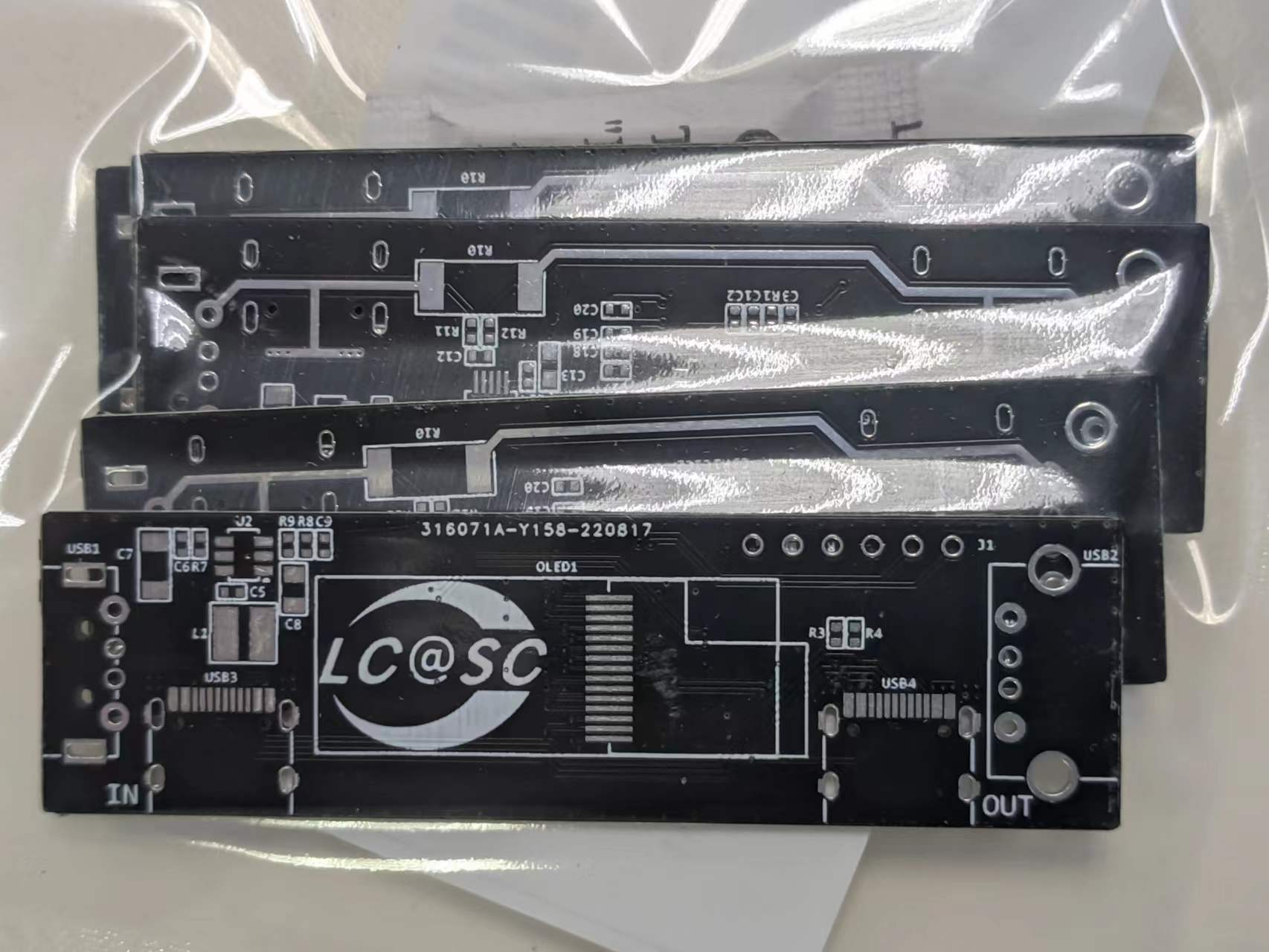
This is a picture of the finished product:

It looks pretty good.

Of course, I still don’t have a USB meter.

BOM download
PCB_PCB_ip6518_2022-09-24.pdf
PCB_PCB_ip6518_2022-09-24.json
PCB_ip6518_2022-09-24.pcbdoc
Gerber_PCB_ip6518.zip
Schematic_Fast charging module based on ip6518_2022-09-24.pdf
SCH_Fast charging module based on ip6518_2022-09-24.json
Sheet_1_2022-09-24.schdoc
61500
SUPERHIFI mp3 based on ac6905a
Introduction: An ordinary mp3
The main control IC is Jerry's AC6905A, which has low power consumption and simple peripherals.
It mainly reads music files through TF cards (actually measured, it can read TF memory cards with a capacity of up to 128G). It is equipped with a Bluetooth function and can output music from Bluetooth through the headphone jack. The audio signal
is equipped with a TP4057 charging chip, with dual lights (yes/no) to indicate charging completion status (although I have never seen this thing light up)

and four-button control, which can switch TF card reading/Bluetooth receiving mode. Pause/play, Next song/volume+, previous song/volume-
toggle switch control switch (seems like nonsense), with power-off memory
PS: Lao Goose (now Love Tomb Style) communication group: 232586710
My communication group: 1092437569
this This is

the video of the finished product at station b: https://b23.tv/5CauV05
BOM download
PCB_PCB_mymp3_2022-09-24.pdf
PCB_PCB_mymp3_2022-09-24.json
PCB_mymp3_2022-09-24.pcbdoc
Gerber_PCB_my mp3.zip
Schematic_MP3 based on ac6905a SUPERHIFI_2022-09-24.pdf
SCH_MP3 based on ac6905a SUPERHIFI_2022-09-24.json
Schematic_2022-09-24.schdoc
61501
Fast charging protocol simulator based on CH224K
Introduction: Use CH224K to simulate fast charging protocol and use the charging head to output multi-level voltage. With output switching function, the output is turned off by default when power is turned on to prevent direct output of high voltage from damaging the equipment.
This chip can be used normally with a DIP switch, but because I have made similar things before, I forgot to turn the DIP switch back after use. As a result, the next time I connected a 5V device, it directly output 12V, and the board instantly malfunctioned. Smoked out, so I decided to make a version like this.
This module is based on CH224K and driven by STM8S003F3P6, realizing the functions of switching voltage and switching output with a single button. And the input voltage can be collected through the ADC, and the flashing frequency of the indicator light can be used to show whether the actual output voltage is the set voltage.
Because CH224K supports up to 20V charging protocol, this causes the Vgs to be up to 20V when using PMOS tubes as switches. The Vgs withstand voltage of small-volume MOS tubes is usually only 12V or 20V. It is difficult to choose small-volume and high-current MOS tubes. This module finally chose an NMOS tube with a voltage resistance of 30V, so that Vgs is only 3.3V. The MOS tube package is PDFN3333. As long as it is a 3x3 size MOS tube, the pin definitions are basically the same. If you are not sure whether it can be used, you can compare the package on the specification sheet.
https://www.bilibili.com/video/BV1w3411x7UA
CH224.zip
BOM下载
PCB_PCB_基于CH224K的快充协议诱骗器_2022-09-24.pdf
PCB_PCB_基于CH224K的快充协议诱骗器_2022-09-24.json
PCB_基于CH224K的快充协议诱骗器_2022-09-24.pcbdoc
Gerber_PCB_基于CH224K的快充协议诱骗器.zip
Schematic_基于CH224K的快充协议模拟器_2022-09-24.pdf
SCH_基于CH224K的快充协议模拟器_2022-09-24.json
Sheet_1_2022-09-24.schdoc
61502
FM1922570CT6-00模块
简介:FM1922570CT6-00模块
参考程序需要搭配这个核心板使用:STM32G030F6P6核心板
模块预留了CS的下拉电阻R4,如果不需要CS功能可以节省一个IO。
模块预留了背光开关,BL引脚悬空或高电平时开启背光,低电平时关闭背光。如果没有关闭背光的需求,可以不焊接Q1、R2和R3,而是焊接R1。
G030_FM1922570CT6.hex
BOM下载
PCB_PCB_FM1922570CT6-00模块_2022-09-24.pdf
PCB_PCB_FM1922570CT6-00模块_2022-09-24.json
PCB_FM1922570CT6-00模块_2022-09-24.pcbdoc
Gerber_PCB_FM1922570CT6-00模块_2022-09-24.zip
Schematic_FM1922570CT6-00模块_2022-09-24.pdf
SCH_FM1922570CT6-00模块_2022-09-24.json
Sheet_1_2022-09-24.schdoc
61503
#第七届立创电赛#基于N32G430的USB功率计
简介:基于N32G430设计,宽输入电压的USB功率计
1、项目功能介绍
基于N32G430的USB功率计
支持4.5~24V宽电压输入
支持测量VBUS线路的电压、电流、功率,同时可以测量D+和D-的电压
2、项目属性
自行设计
3、开源协议
CC-BY-NC-SA 3.0
4、硬件部分
MCU采用国民技术N32G430K8L7,LQFP32封装。
监测芯片采用德州仪器INA226,最大支持36V输入电压。支持测量电压和电流,并自动计算功率。使用I2C输出测量结果。
数字电源采用DC-DC方案,为MCU和OLED供电。DC-DC的高效率可以防止高压差时PCB发热,影响测量结果。芯片选用TMI3359,最大支持30V输入电压。采用CD32封装的4.7uH电感,保证电感不会发热。我个人喜欢开关频率较高的DC-DC,这样可以选择较小的电容和电感,减少电路的面积。
模拟电源采用LDO方案,为INA226供电。LDO的输出电压波动更小,更适合精密的测量。另外INA226属于低功耗元件,即使压差比较大,也不会发热。芯片选用SE8533,最大支持36V输入电压。
输入电容采用耐压50V的MLCC电容。因为MLCC是陶瓷材质电容,会随着电压升高发生一定形变,导致容量降低,所以,MLCC的耐压值一般选用最大输入电压的2~3倍。
电流采样电阻的阻值为10mΩ,较小的阻值可以尽量降低在这个电阻上产生的压降。较低的温度系数可以保证在电流较大时电阻的阻值变化较小,提高测量的线性度。本次选用的电阻为1%精度、2W功率,温度系数为±70ppm/℃。
显示屏使用0.91寸OLED屏,分辨率为128x32,通信协议为SPI。
接口方面,输入端为一个USB-A公头和一个USB-C母头,输出端为一个USB-A母头和一个USB-C母头。使用USB-A可以免去数据线,而两个USB-C则考虑到了PD协议以及使用中可能需要延长线将功率计放置于利于观察的位置。
焊接完成的PCB如下图所示。
正面

背面

INA226特写

N32G430特写

5、软件部分
由于不需要非常精确的时钟,所以本次采用HSI作为时钟源,节省成本。
由于不需要大量运算,所以未开启PLL功能,降低了系统的总功耗。
系统外设主要使用了SPI、I2C和ADC。其中,I2C用于INA226的通信,SPI用于OLED的通信,ADC用于采集D+和D-的电压。
本次软件开发使用Nations.N32G430_Library.1.0.0
外设的使用参考了其中的examples
6、BOM清单

7、大赛LOGO验证
8、演示您的项目并录制成视频上传
正常工作效果展示

20V输入展示
使用一加手机充电器,配合CH224K产生20V电压,没有连接负载,功率计工作正常。

小米27W快充协议从开始到稳定实测视频
studio_video_1663516034934.mp4
studio_video_1663515771172.mp4
studio_video_1663515548238.mp4
N32G430_USBTester.hex
BOM下载
PCB_PCB_#第七届立创电赛#基于N32G430的USB功率计_2022-09-24.pdf
PCB_PCB_#第七届立创电赛#基于N32G430的USB功率计_2022-09-24.json
PCB_#第七届立创电赛#基于N32G430的USB功率计_2022-09-24.pcbdoc
Gerber_PCB_#第七届立创电赛#基于N32G430的USB功率计.zip
Schematic_#第七届立创电赛#基于N32G430的USB功率计_2022-09-24.pdf
SCH_#第七届立创电赛#基于N32G430的USB功率计_2022-09-24.json
Sheet_1_2022-09-24.schdoc
61504
具有DC-DC供电的STLink V2.1/DAPLink
简介:DAPLink调试器,使用USB-C接口,引出SWD、UART、SWO和MCO引脚
If you think the ST-Link V2.1 onboard the Nucleo is inconvenient to use, you can transfer the ST-Link V2.1 part to the PCB of this project, so that you get an ST-Link V2 with a USB-C interface. .1.
Because DAPLink uses the same pin definition as ST-Link V2.1, this project can also be used as DAPLink.
It has a red and green two-color indicator light, and the serial port has an independent indicator light, so the firmware in the attachment disables the indicator light flashing function when sending and receiving data on the serial port.
The Reset button is connected to the Reset output of the SWD. Therefore, when the debugged target board does not have a reset button but has a reset pin, this button can be used to reset. In addition, when you need to upgrade the DAPLink firmware, press and hold this button to power on to start from the Bootloader.
This project uses DC-DC power supply, and the 3.3V output can provide larger current.
The MCO function drawn from the side is an 8MHz clock signal output, and the clock source is an 8MHz crystal oscillator. When debugging a target board without a crystal oscillator, connecting the MCO to the clock input pin of the target board can provide a relatively accurate clock source.
The SWO function has not been tested yet.
This project uses 0603 package resistors and capacitors, which is more convenient for novices to practice welding.
DAPLink firmware.zip
PCB_PCB_2020-10-14_16-31-05_2022-09-24.pdf
PCB_PCB_2020-10-14_16-31-05_2022-09-24.json
PCB_2020-10-14_16-31-05_2022-09-24.pcbdoc
Gerber_PCB_2020-10-14_16-31-05.zip
Schematic_STLink V2.1 with DC-DC power supply_DAPLink_2022-09-24.pdf
SCH_STLink V2.1 DAPLink with DC-DC power supply_2022-09-24.json
Sheet_1_2022-09-24.schdoc
61505
STM32G030F6P6 core board
Introduction: Click screen artifact?
It is recommended to use this debugger: STLink V2.1/DAPLink
STM32G030 series with DC-DC power supply is no longer overpriced and is a qualified substitute for STM32F030. It has a higher main frequency and several more IOs.
I accidentally discovered that the STM32G030 has two IOs that can be used as both SPI and I2C, so I decided to make an interface to facilitate debugging of various modules, and this is the core board.
All pins of this core board lead to two pads, which allows for more flexible wiring. Of course, you can also solder only one row of pins and use the other row as test points.
The core board has a power indicator light, a custom function indicator light, a reset button, and I2C pull-up resistor. Indicators connected to GPIO as well as I2C pull-up resistors can be enabled or disabled using jumper caps.
The core board leaves PA0~PA7 floating (PA2 and PA3 can also be used as serial ports for outputting debugging information) to facilitate debugging of parallel interface peripherals.
Both CC1 and CC2 of the core board are connected to 5.1k pull-down resistors to ensure that the PD protocol adapter can also be powered normally.

BOM download
PCB_PCB_STM32G030F6P6 core board_2022-09-24.pdf
PCB_PCB_STM32G030F6P6 core board_2022-09-24.json
PCB_STM32G030F6P6 core board_2022-09-24.pcbdoc
Gerber_PCB_STM32G030F6P6 core board.zip
Schematic_STM32G030F6P6 core board_2022-09-24.pdf
SCH_STM32G030F6P6 core board_2022-09-24.json
Sheet_1_2022-09-24.schdoc
61506
Vllink Lite Pocket Edition
Introduction: A simplified version of Vllink Lite, retaining SWD and UART functions and reducing the PCB area. Using GD32F350G8U6 solution
First of all, thanks to Vllogic for the open source Vlllink Lite firmware.
The author's open source address is https://gitee.com/vllogic/vllink_lite
or https://github.com/vllogic/vllink_lite.
This design is a simplified version of Vllink Lite. In order to reduce the size, only the SWD and UART functions are retained.
Vlllink is transplanted using DAPLink source code and retains the functions of DAPLink. But it is implemented using a smaller package and lower price MCU. This design uses GD32F350G8U6, which is only 4x4mm in size, and does not require an external crystal oscillator.
This design uses the more common USB-C interface, making it easier to find a suitable data cable.
For specific usage methods, please refer to the original author's Github, which has detailed introduction and usage methods.


BOM download
PCB_PCB_Vllink_Lite_GD32F350G8_2022-09-24.pdf
PCB_PCB_Vllink_Lite_GD32F350G8_2022-09-24.json
PCB_Vllink_Lite_GD32F350G8_2022-09-24.pcbdoc
Gerber_PCB_Vllink_Lite_GD32F350G8_2022-09-24.zip
Schematic_Vllink Lite Pocket Edition_2022-09-24.pdf
SCH_Vllink Lite Pocket Edition_2022-09-24.json
Sheet_1_2022-09-24.schdoc
61507
ES2Eds3 ESP32S3 WiFi Development Board
Introduction: Based on ESP32S3 WiFi development board, onboard OTG and UART, automatic download, DCDC, ESP32 S3
# ES2Eds3 ESP32S3
ES2Eds3 ESP32S3 WiFi development board
## Function
* Automatic download
* OTG
* BOOT/EN button
* Onboard UART chip
* No LED
* It should not be plugged into the breadboard
##### v1.0 only changed Silk screen and ESD will not be verified
##### v0.9 verification completed
! [QQ screenshot 20211230154408.jpg]

![QQ screenshot 20211230154603.jpg]

###### The automatically downloaded transistor is used up
! [QQ screenshot Screenshot 20211230154615.jpg]

- - -
BOM download
PCB_PCB_ESP32S3FN8_2022-09-24.pdf
PCB_PCB_ESP32S3FN8_2022-09-24.json
PCB_ESP32S3FN8_2022-09-24.pcbdoc
Gerber_PCB_ESP32S3FN8.zip
Schematic_ES2Eds3 ESP32S3 WiFi Development Board_2022-09-24.pdf
SCH_ES2Eds3 ESP32S3 WiFi Development Board_2022-09-24.json
Sheet_1_2022-09-24.schdoc
61508
electronic


 京公网安备 11010802033920号

 IDT7205S30D


