The overall hardware block diagram of the system is
shown in the figure below. The main controller uses an STM32L051K8U6, the battery-powered design uses a TPS63020, and the display uses a 1.54-inch 200*200 e-ink screen. If you don't want to buy an e-ink screen, or want a very long lifespan, you can use an ultra-low power version that only uses LEDs for display. Card information is stored entirely in the MCU's internal EEPROM.
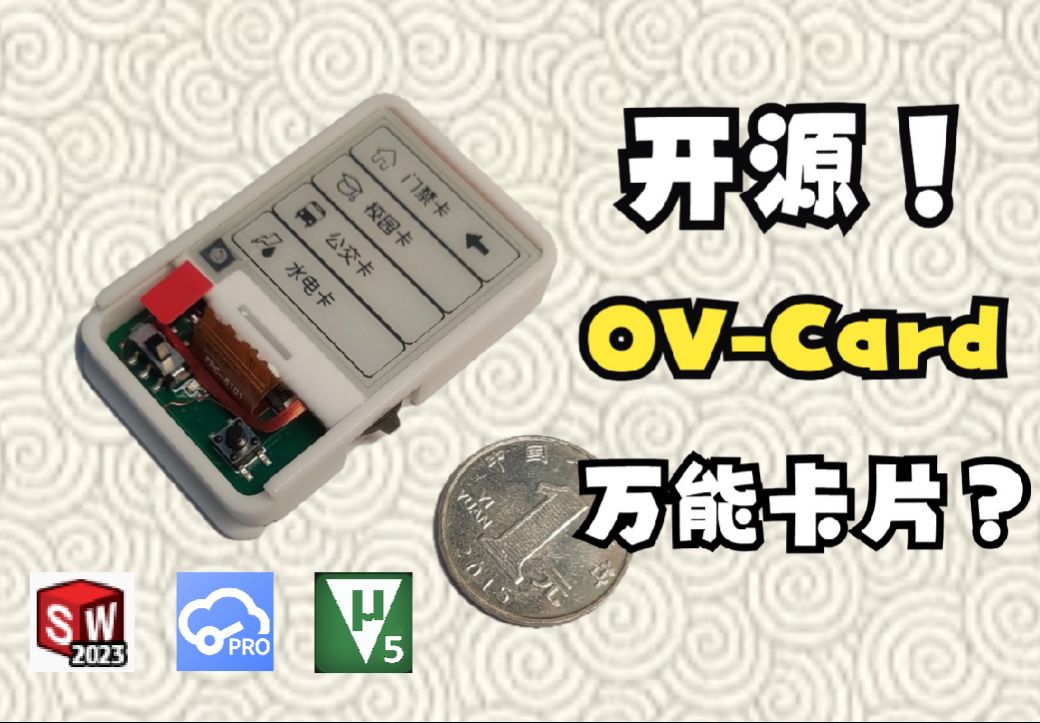
Note that the RC522 supports 14443; this design uses only one UID card and the RC522 to implement the card emulation mode.

Instructions for Use
! **Note:** Please switch the mode before powering on. Do not slide the switch to switch modes while the power is on!
**Hardware Operation Instructions:
** 1. Press the button to power on; release to power off.
2. Use the dial switch to switch the selected position (i.e., switch cards) by sliding it up and down after powering on.
3. Switch modes by sliding the switch. (Do not switch modes while powered on)
Mode switching instructions:
1. Slide to the left for copy mode. After power-on, you can copy external cards to the selected storage location. For example, if an access card is selected, simply bring the external card close to the back to write the card information to the selected storage location.
2. Slide to the right for card emulation mode. After power-on, the information is written to the IC card. As long as the slide switch remains on the right, the card can still be swiped after power-off, meaning it can be read by an external card reader.

The design principle
uses the RC522 because it supports IEC 14443A/MIFARE. Its supported functions are as follows: it has card read/write mode, but does not support card emulation mode. Therefore, this design uses an external UID card, enabled, to implement card emulation mode.

The functional block diagram and IC card information partition diagram are shown below. The NFC module reads the card number of the external IC card (i.e., the data in sector 0, block 0) through the RC522 and then stores it in the EEPROM inside the STM32L051. The sliding switch controls the opening and closing of the coil of the internal UID card, thus adding an enable function. Through the NFC module, the card number information stored in the EEPROM is written into the UID card, achieving the card copying function.
Generally, copying the information of sector 0, block 0 is sufficient, such as access cards, campus cards, and water cards, which all identify the card number information of sector 0, block 0.


Hardware Specifications:
1. A CR1220 battery is used. For a more environmentally friendly approach, a rechargeable ML1220 can be used, which can be recycled after use.
2. The power supply section uses a TPS63020. Since the current is much less than 10mA, the TPS63020's power save mode is used. If a TPS63021 is used, the feedback resistor needs to be modified according to the schematic diagram.
3. On the PCB, the via below the sliding button is used to solder the coil, as shown in the figure below. The reason for not drawing another coil on the PCB is that the RC522 coil in the NFC section is too close to the UID card coil, making it undetectable and unable to read or write. Previously, I tried drawing the UID card coil in inner layer 1, but NFC couldn't read or write it.

The software
documentation has two versions: a normal version with an e-ink screen, and a low-power version adapted for LP boards, replacing the e-ink screen with LEDs.
If you need to change the image displayed on the e-ink screen, you can directly use image-to-model conversion. Here you can use Image2Lcd, set as shown below

. In ImageData.c of the .BSPEPaper file, change the gImage array as shown below .

Other notes :
When printing on the LP low-power board, you can modify the silkscreen printing yourself, placing it under each LED.
Users who are interested can modify the e-ink screen interface image themselves. Image to LCD model conversion is sufficient.
Caution: Never copy other people's cards, only copy your own cards. Be a good citizen!
Demo
video link: https://www.bilibili.com/video/BV1Ju4y1q766
The repository link
contains all the hardware, software, and 3D printed shell materials.
GitHub repository: https://github.com/No-Chicken/OV-Card
QQ group
: 572216445

Bottom cover parts.STL
Shell parts.STL
code project.rar
PDF_Universal Card OV-Card.zip
Altium_Universal Card OV-Card.zip
PADS_Universal Card OV-Card.zip
BOM_Universal Card OV-Card.xlsx
90709
Mini CNC Power Supply - FL Power V3
This is a mini power supply, measuring approximately 53x53x17 (mm), featuring buck-boost output and USB power metering. Latest version V3.

Project Parameters
: Dimensions: 52x52x16mm (Width x Length x Height)
Interaction Method: 1.54-inch 240x240 resolution TFT screen, 1 rotary switch, 2 tactile switches
Power Input Interface: Type-C port (supports PD protocol), XT-3.0 male connector, 4mm banana plug interface (3D shell optional)
Power Output Interface: Power metering port Type-C, adjustable power output XT-3.0 male connector, 4mm banana plug interface (3D shell optional)
Adjustable Power Output Range: 0.4-35V, 0-5A
USB Power Metering: PD protocol detection, QC protocol
Open Source License
: This project is licensed under the "CC-BY-NC-SA 4.0" Creative Commons Attribution-ShareAlike license. Commercial use is prohibited. Please indicate the source when reprinting.
Open Source Code: https://gitee.com/yllff/flpower
Project Attributes:
This project is being publicly released for the first time and is my original work. This project has not won any awards in other competitions.
Project Update
2024/4/2: Added some introductory content and updated the Core V2.1 board.
【【Open Source】Mini CNC Power Supply (Part 1) 【Daily Fun for Electronic Engineers】】
The Core V2.1 board has replaced the encoder, adopted a pulsator switch to reduce costs, and brought out the SWD port and serial port. This is for future feature additions. Note that this version is incompatible with previous casings. Code is compatible.
Added some circuit and code descriptions.
2024/11/10: Updated the Core V3.0 board, Power V3.0 board, and Panel V3 acrylic panel.
【【Open Source】Does My Brother Have a Girlfriend? Do You Mind Having Multiple Watches? ?】
Updated the entire structure, redesigned the internal PCB board,
readjusted the code architecture, updated the UI interaction, and ported Cherry USB, Cherry DAP, and other code to implement virtual serial ports and DAPLINK.
2024/11/13: Supplemented documentation.
2024/11/17: Supplemented documentation.
U21 and U22 on the core board and U21 on the power board are not feedthrough capacitors; they are used for shorting! Some replica builders have already fallen into this trap!
After burning the firmware to the board, it needs to be connected to a PC to import calibration coefficients. Please refer to the attached video.
Power board C7 and C8 have been changed to 20pF; the project files have been updated.
Updating features include:
VCP virtual serial port function (implemented in version V3.0)
, ammeter measurement (implemented in version V3.0)
, DAPLink function (implemented in version V3.0)
, 0-50V waveform sampling channel (this function will be removed)
, 2S battery base module for scenarios without external power supply
, and 4S battery base module for constant current and constant voltage charging of the battery in scenarios without external power supply
(to be implemented).
Project Introduction:
1. The hardware
PCB board consists of two parts: a core board and a power board. They are connected by double-row pins and fixing nuts, and the layout takes into account the height of the PCB stack-up. The core board is a 4-layer board, and the power board is a 2-layer board, with resistors and capacitors primarily using 0603 packages. The main controller is the Arteli AT32F403ARGT7, an Arm Cortex M4 core, 1MB Flash, 96K RAM, and a 240MHz clock speed. It provides three power input methods: Type-C, XT30, and a 4mm banana plug. The built-in FUSB302 enables PD protocol detection. The adjustable power control chip is the SC8701, which can achieve buck-boost output. This design broadens the application scenarios; for example, if only a 5V power supply is available, it can output 2-30V. Alternatively, it can be used with 18650 batteries in scenarios without an external power source. The USB power meter and adjustable power input interface share the same Type-C interface.

1.1

When the frame is used as a power supply, the power is connected to the DCIN (Type-C port) of the core board. If it is a charger with PD protocol, it can be tricked into maximum power mode via FUSB302 (I used a 20V 4.5A charger in my test), and then connected to the power board through the studs between the two PCB boards. The control signals of the core board are connected to the power board through a dual-row header.
The board has compatibility design; there are two shorting points on the core board and one shorting point on the power board. In this version, the shorting method of the power board is as follows:

The shorting method of the core board is as follows:

1.2 The structural
shell adopts an integrated middle frame plus a base plate and an acrylic panel structure. The acrylic panel can protect the LCD screen to a certain extent. I still designed two sets of drawings: 3D printed and CNC aluminum alloy. The 3D printed shell size is 53x53x16mm, and the aluminum alloy shell size is 52x52x16mm. In addition, when designing the PCB size, I considered the size of an aluminum alloy profile, which should be more suitable, but it has not yet been verified. I will wait until JLCPCB adds CNC technology to the profiles next year.
The 3D printed shell has four screw fixing points on the middle frame. The base plate is directly fixed to the PCB board and designed to be flat. It is best to use metal material for heat dissipation. It is recommended to apply thermal conductive silicone to the MOSFET to ensure full contact with the base plate. After the two PCBs are connected, they are fixed to the middle frame through solder terminals on the power board. The advantage of this type of shell (nylon material is recommended for its high temperature resistance) is that it is much cheaper than the cheaper CNC. The disadvantage is that it is a bit soft after printing. Compared with the first version, the middle frame structure is more beautiful and sturdy, and the separation of the base plate can increase heat dissipation.

The shape of the CNC aluminum alloy shell is shown in the figure below, and it is fixed by four screws at the bottom. The advantage of this type of shell is that it has a good texture and hardness, which accelerates heat dissipation. The disadvantage is that it is expensive! Also, pay attention to the connection of the shell to GND!

1.3 Principle Analysis
1.3.1 Core Circuit Power Supply Design
The core part of the mini power supply can be powered through the power supply side (USB2) or through the debugging USB port. When both are powered at the same time, the power supply from the debugging USB port side will be selected through the power switching circuit. The power switching circuit is shown below. Let's analyze it briefly. First, when the power supply is on, U11 (ME3115AM6G) outputs VCC1 with a voltage of 3.7V, which is then output to VCC through the body diode of Q5. Simultaneously, because the gate of Q5 is grounded through R27, the drain and source are connected, reducing the power consumption caused by the voltage drop across the body diode of Q5. At this time, 3.3V is obtained through U10 (ME6211A33M3G-N). When power is plugged into the debugging USB port, the EN pin of U11 is pulled low because it is connected to the GND pin of the debugging USB port, and VCC1 becomes 0V. At the same time, the gate of Q5 has a voltage of 5V, while the source of Q5 is approximately 4.4V due to D3. Since Vgs > 0, Q5 is cut off. In this case, VCC is powered solely by VCC2. The advantage of this circuit is that when powered from the power supply side, there is little loss due to the conduction of Q5. Furthermore, when both power supplies are applied simultaneously, the power supply to the power supply side can be shielded, eliminating internal circuit losses and facilitating accurate calculation of the losses in the input and output sections of the CNC power supply.

1.3.2 Adjustable Voltage Design
The hardware utilizes the SC8701 power control chip, a synchronous 4-power transistor Buck-Boost controller. Its output voltage can be higher, equal to, or lower than the input voltage, significantly saving overall space. This chip also provides current limiting protection. Its main characteristics are an input voltage range of 2.7V to 36V and an output voltage range of 2V to 36V, adjustable via a PWM signal. A drawback is that the minimum adjustable output voltage is only 1/6 of the maximum set voltage. That is, if the maximum output voltage is designed to be 30V, the minimum adjustable output voltage is 5V. This is because when the PWM output is 0, Vout = 1/6 Vset.

So, is there a way to widen the adjustable range of the output voltage? The answer is yes. We can solve this from another angle by keeping the PWM control pin output high and adjusting the resistor at the FB pin. According to the formula in Figure 6, we know that the resistance values of Vout and RDown are inversely proportional. If we keep the PWM control pin high, that is, let the SC8701 output the maximum set value Vout_set, then changing RDown will also change the output voltage.

However, we need to use an MCU to control the output, so we need to design a circuit. The Air32f103cct6 has a DAC function, but the 12-bit resolution is not enough. The circuit in the figure below can be used to convert the 16-bit resolution PWM signal into an analog signal and convert the voltage range to 0-V_REF.

The DAC signal is connected to the FB point through a resistor. By adjusting the amplitude of the DAC signal, the output voltage can be set. The principle analysis is as follows: when the DAC output is 0V, the current flow is as shown in the figure below. The two resistors are equivalent to parallel connection, and the maximum output voltage Vo is 1.22*(1+100k/((6.2k+2k)/2)), which is about 30.97V. The actual test is about 30.2V, mainly due to the error in the resistance value.

When the DAC output is the reference power supply (2.5V), the current flow is shown in the diagram below. The current flowing through R23 is almost 0A because after voltage division, the voltage at point FB is already 1.22V. Ideally, the SC8701 will not output any voltage, Vo=0V. Actual testing shows approximately 1.4V, mainly due to the instability of the reference power supply and resistance errors. Therefore, when the output DAC voltage is in the range of 0-2.5V, the ideal output voltage range is 0-30.9V, thus achieving a wide voltage output range. The SC8701 is labeled as having an output of 2-36V in the documentation; however, the internal workings have not been thoroughly investigated, and it is uncertain whether the minimum output is 2V.

2. The
MCU software code is divided into two parts: bootloader and app. The bootloader provides a simulated USB drive drag-and-drop upgrade function, allowing for app firmware upgrades without additional software tools, which is quite convenient. The app code is based on FreeRTOS+LVGL, the IDE uses Keil 5.38, and the GUI is generated using SquareLine Studio. The bootloader firmware is downloaded via Keil or JFlash.
2.1 Application Firmware Update:
After flashing the bootloader firmware, the application firmware can be upgraded easily. The specific steps are: first connect one end of the USB cable to the computer, then press and hold the '<' key on the mini power supply and insert the other end of the USB cable into the debugging port. The computer will then eject a USB drive named "FL POWER". Open the USB drive; it will contain a TXT file named "READY". Drag and drop the firmware file to be updated (bin or hex format) into this USB drive. The USB drive will be re-recognized, and the "READY" TXT file will be updated. "SUCCESS" indicates a successful update.
2.2 GUI Interface
: The interface is generated using SquareLine Studio, a visual drag-and-drop UI editor that allows for quick and easy creation of beautiful graphical user interfaces for embedded and desktop applications. Official website: https://squareline.io/. It is free for personal use after download and installation, but is limited to designing only 5 UI interfaces and placing 50 controls. Simple software settings allow for easy and intuitive implementation of animation effects.
2.3 Debugging Host Computer
: The host computer is compatible with the previous soldering station and currently allows for parameter setting and calibration. The power supply connects to the PC via USB, enabling virtual serial communication.

2.4 Code Analysis
2.4.1 App Application Code
The app code is based on FreeRTOS + LVGL. After BSP initialization, multiple Tasks are created, as shown in the figure below.

Task_sample mainly collects and calculates the voltage and current values of each channel, task_gui is responsible for LVGL operation, and task_pd is used for PD protocol communication of the power port to obtain the maximum power voltage option, as shown in the figure.

2.4.2 Bootloader Code
The bootloader side code is mainly used for firmware upgrades. When the mini power supply is connected to the computer via USB and the corresponding button is detected as pressed, the upgrade stage begins. The code creates a FAT16 file system and simulates a USB flash drive using the chip's internal Flash (starting from 0x08004000) for storage. The firmware to be upgraded can then be dragged and dropped into the USB flash drive, and the firmware will be copied to the chip's internal Flash. After completion, the power supply is restarted. If no corresponding button is detected after power-on, the process jumps directly to the App application code and executes it. The Main function code is shown in the figure below.

3. Assembly
: Assembly is relatively simple; this section only describes CNC structure assembly. First, connect the two PCBs. Place two button caps inside the middle frame, then place the PCBs into their corresponding positions on the middle frame. Apply thermal paste to the MOSFETs on the back of the power board, and then cover with the base plate and secure with screws. Note that the leads of the through-hole components on the back of the power board need to be flattened to prevent short circuits from contacting the casing.

4. Functions [See video link for details]
4.1 The CC meter
is connected to the circuit via two Type-C ports to detect voltage, current, power, etc. It can display waveforms, supports PD protocol detection, and has adjustable PPS output.
4.2 Buck-boost output :
Supports multiple power supply connection methods. The input voltage range supports 5-32V and has reverse connection protection. The XT30 interface outputs an adjustable voltage of 0.4-35V and an output current of 0-5A.
4.3 I/O expansion functions:
Expandable functions are achieved through the USB port and two 4-pin terminals, such as DAPLINK, dual serial ports, etc. The interface will display the relevant configuration data.

5. Usage and Testing
5.1 Usage Introduction
After PCB assembly, the firmware is first burned in. Currently, it is burned in using a J-Link or similar program via the reserved SWD port on the core board. After burning, connect to the PC via USB and update the calibration parameters using the host computer (downloadable in the attachment). Generally, you need to manually recalibrate the input voltage and current, output voltage and current, and the corresponding voltage of the output PWM.
The power supply has 3 Type-C ports and 1 XT3.0 port, 2 buttons, and 1 pulsator switch. Their uses are shown in the diagram below. Currently, the focus is on simplifying operation as much as possible for the CNC power supply function; button functions may be modified as more functions are added later.


USB Communication Port: Used to connect to a PC to upgrade application firmware and as a separate power supply for the ammeter timing to eliminate internal loss errors. Also used to connect to the host computer software.
Power Input Port: Connects to a 5-32V power supply. Various charging heads can be connected via the Type-C port, or other power supplies can be connected from the XT30. The maximum power setting is selected by default via the PD protocol.
Indicator Lights: Dual-color indicator lights. Blue indicates the breathing light mode is running, which may be used for status indication later. Red indicates DAPLINK connection to a device.
Ammeter Function Output: Directly connected to the power input port, used as an ammeter for timing. Note that the voltage at this port also increases after the input power is boosted via the PD protocol! Caution is required when using external power supplies!
CNC Power Output: 0.4-35V output, XT3.0 interface. Note the positive and negative directions!
Rotary Switch: Switches between menus, focuses controls, and modifies parameters.
Right Function Key: Short press to switch interfaces in the current application; long press to return to the main menu.
5.2 Load Ripple [Version 2.0, Version 3.0 not thoroughly measured]
Waveforms at various load stages. Due to the maximum power of the input power supply being 60W (20V 3A), the maximum output was only measured at 30V 2A.

[5V no-load]

[30V no-load]

[3.3V 3A]

[5V 3A]

[15V 3A]

[30V 2A] The project
references
some code from the following authors. I greatly admire their open-source spirit and am very grateful to them!
Hezhou Official Repository: https://gitee.com/openLuat/luatos-soc-air32f103
STM32 USB Flash Drive Upgrade Firmware: https://gitee.com/joeylolipop/stm32-iap-msd
FUSB302 PD Protocol: https://gitee.com/liuzewen/PD_Micro
Cherry USB: https://github.com/cherry-embedded/CherryUSB/
Cherry DAP : https://github.com/cherry-embedded/CherryDAP/
Cherry RB: https://github.com/cherry-embedded/CherryRB
LCSC DAPLINK Debugging Tool: https://oshwhub.com/li-chuang-kai-fa-ban/li-chuang-daplink-diao-shi-gong-ju
Other
main code is still being organized and will be submitted to Gitee later.
Open Source Code: https://gitee.com/yllff/flpower
QQ Discussion Group: 334607120
Important!
1. When prototyping, select 1.0mm thickness for both PCBs! 1.0mm thickness! 1.0mm thickness!
2. The component parameters in the schematic have been basically checked, but it's best to double-check them when generating the list.
4. The V3 version's main controller is AT32F403AGT7!
5. All parts (casing, front panel, PCB) have been modified in the V3 version, please note!
6. U21 and U22 on the core board and U21 on the power board are not feedthrough capacitors, they are used for shorting!! Some replica makers have already fallen into this trap!!!
V1.0 Data.rar
v3 firmware without MSD file.rar
V3 outer casing.rar
v3 source code.rar
FL Power Calibration Coefficient Import.mp4
HeaterAssist.rar
PDF_Mini CNC Power Supply - FL Power V3.zip
Altium Mini CNC Power Supply - FL Power V3.zip
PADS_Mini CNC Power Supply - FL Power V3.zip
BOM_Mini CNC Power Supply - FL Power V3.xlsx
90710
[First Release Online] ZYNQ7035 Core Board and High-Speed ADC
This project plans to open-source the ZYNQ7035 core board and an 8-bit 1GSPS 4-channel ADC module. The 7035 core board and high-speed ADC are geared towards high-speed communication and high-speed electronic measurements such as a 1GSPS 4-channel oscilloscope.
This project
aims to open-source the ZYNQ7035 core board and an 8-bit 1GSPS 4-channel ADC module. The previous project, featuring a 7020 core board and RF module, was geared towards general applications and electronics design competitions; this 7035 core board and high-speed ADC are geared towards high-speed communication and high-speed electronic measurements such as a 1GSPS 4-channel oscilloscope. The ZYNQ7035PS side uses a dual-core Cortex-A9, while the PL side is based on the Kintex-7 architecture, which is superior to the Artix-7 architecture of the 7020 and
7010, offering stronger timing control capabilities. The PL side has 275k logic cells, more than three times that of the 7020 and nearly ten times that of the 7010. The DSP resources are more than four times that of the 7020, allowing for steeper filter designs and the deployment of larger-scale DSP algorithms. Simultaneously, the BRAM resources are more than three times larger than the 7020, enabling the ILA to capture more data and facilitating debugging.
Compared to the ZYNQ7035 which costs 3000-4000 yuan on TB, the core board BOM cost of this open source is only a few hundred yuan, which provides strong help to electronic enthusiasts who need ZYNQ7035. Moreover, this project is the first open source 7035 on the oshwhub platform, and it seems to be the first one on the entire network!


Of course, in addition to the ZYNQ7035 core board, this project will also open source the HMCAD1511 8bit 4-channel 1G sampling rate high-speed ADC module and driver.

The open source agreement
is prohibited for commercial use without the author's permission. Reprints or citations must indicate the original author and project link.
Project related functional
resources introduction:
(1) ZYNQ7035 core board PS end: Onboard 1 DDR3, QSPI FLASH, SD card adapter chip, Gigabit Ethernet, JTAG, UART.
(2) TYPEC Port Description (Important!!): Using the FT2232 chip, single-chip JTAG+UART operation is completed. The USB port uses TYPEC, which includes ESD+common-mode filtering and an ideal diode to prevent reverse current flow. No more debugging, power supply, programming, and connecting a bunch of wires (even various old USB interfaces...). One TYPEC is enough! A boon for developers~
(3) Power Management: The core power supply used in this project is Vishay's SIC431, which features remote sampling, high efficiency (97% peak efficiency), and 24A power supply capability. Furthermore, this device is internally compensated and does not require an external ESR network to achieve loop stability. The auxiliary power supply is TPS82130, our old friend :) The power-on sequence is shown in the figure

(4) ZYNQ7035 core board PL end: The PL end leads out a group of GTX BANK; 36 pairs of differential equal length High Performance BANK with a level of 1.8V; 35 pairs of differential equal length High Range BANK with a level of 3.3V, a total of 158 IOs. Due to the limitation of the 6-layer board, no more IOs are led out, but it is enough for use.
(5) ZYNQ7035 baseboard: This time, a matching baseboard was open sourced, in which HRbank is led out as PMOD interface (PMOD is good civilization!), HPbank is led out as BTB connector. The PS end is given an Ethernet interface, two 2510 power supply ports, an SD card interface, an LDO to power PMOD, and a power protection IC: with fast overvoltage clamping, adjustable overvoltage lockout, adjustable current limit, adjustable output slew rate control and overheat protection. Since there is no equipment for testing GTX at the moment, the baseboard does not have GTX pins. You can draw it yourself if needed.
(6) HMCAD1511: 8-bit 1GSPS ADC, analog front-end is LMH6521 high-performance dual-channel DVGA, -3dB bandwidth is 1.2GHz. Input impedance is 50Ω, programmable gain, dynamic range is 31.5dB, step size is 0.5dB. Onboard phase-locked loop HMC832 provides sampling clock. The interface uses 1.8V LVDS. Onboard power management uses integrated DCDC and ultra-low noise ultra-high PSR LLDO, and uses feedthrough capacitor filtering. The input is 5V 2510 interface.
Project attributes
This project is being published for the first time and is my original project. The project has not won any awards in other competitions.
Project Progress
(I) ZYNQ7035 Core Board:
(1) ZYNQ Chip: Normal operation, VIVADO normal connection:

(2) DDR3: Normal operation, 0 errors:

(3) JTAG+UART: FT2232 normal operation, JTAG and UART can be used normally.
(4) Ethernet: RTL8211 normal operation, network loopback test results:

(5) Firmware and Startup: QSPI FLASH firmware results, offline startup results:

(II) HMCAD1511:
Normal operation, Figure 1 shows the data test mode, and it can be seen that all channels are working normally. Figure 2 shows the ILA data acquisition data imported into MATLAB for processing, and the FFT and time domain waveforms are shown in the figure.


Design Description
I. ZYNQ7035 Core Board:
(1) Power Supply Section: The core power supply uses Vishay's SIC431, with a maximum output current of 24A; the auxiliary power supply uses a TPS82130 integrated inductor DCDC converter, which can output a maximum current of 3A, with a total of 6 voltages. The power-on sequence is 1V0->1V8->1V2&2V0->1V5&3V3. For detailed parameters and requirements, please refer to the Xilinx official manual.

The core power supply test result is 999.5mV with an error of 0.5 per thousand. The ripple is 8mV peak-to-peak and 500uV effective value, which meets the Xilinx official requirements.

(2) DDR3: DDR3 uses Micron's single-chip MT41K256M16 4Gbit.

(3) FLASH: QSPI FLASH uses W25Q256JVEIQ (or W25Q128JVEIQ)

(4) SD card adapter: SD card adapter uses TI's TXS02612RTWR
(5) Ethernet: Ethernet uses REALTEK's RTL8211

(6) Clock: PS uses a 33.3333MHZ 20ppm active crystal oscillator, PL uses a 100Mhz 20ppm active crystal oscillator. GTX uses a 125MHZ differential crystal oscillator (LVDS)
(7) JTAG+UART: Uses FT2232HQ, a single chip completes two tasks.
(8) Board-to-board connector IO resources: A set of GTX BANK is brought out from the PL end; 36 pairs of differential equal-length High Performance BANK with a level of 1.8V; 35 pairs of differential equal-length High Range BANK with a level of 3.3V, for a total of 158 IOs. PS leads to ETH, SD card, JTAG, and other pins can be implemented using PL pin resources through EMIO if needed.
(9) Boot mode selection: Three boot modes are provided, namely JTAG boot, QSPI FLASH boot, and SD card boot. Changes can be made through the DIP switches on the core board:
Boot mode
Switch 1
Switch 2
JTAG Start
ON QSPI FLASH Start ON
OFF SD Card Start OFF OFF ( 10) ZYNQ chip model: XC7Z035-FFG676, XC7Z035-2FFG676, XC7Z030-2FFG676, XC7Z030-FFG676 Software description (1) ZYNQ7035 provides UART, RGBLED, DRAM, Ethernet test projects (see attachment), VIVADO version is 2022.1 (2) HMCAD1511 driver project is zynq Ultrasale +MPSOC XCZU3EG (interface definition compatible with ZYNQ7035 baseboard, porting required) see attachment, VIVADO version 2022.1. Physical demonstration design notes: (I) When soldering the Zynq core board, it is recommended to solder the power supply first, test the power supply voltage and startup sequence to ensure they are normal, and then solder the feedthrough capacitors and other chips to prevent chip damage due to abnormal power supply. (II) When soldering the ZYNQ7035 chip with the steel cover, it is recommended to use a BGA soldering station, not a hot air gun, or choose JLCPCB SMT to directly mount it. (III) Suggested soldering order: power supply - BGA chip - front peripheral circuit - back capacitors and resistors - connectors. (IV) After soldering, you can verify by burning the RGBLED test program in the attachment. (V) FT2232HQ program burning: Note that changing FT2232 to JTAG+UART requires program support and cannot be used without burning. For Vivado 2022, it comes with built-in support for FT2232. The program can be burned by following these steps: (1) Open Vivado (any project) and connect the core board to the Type-C port (plug in the cable). (2) Open Device Manager to check if there is a new USB device inserted. If not, it means there is a hardware problem. Normally, as shown in the figure, it indicates that there is a USB Serial A and B connection. (3) Open Vivado's TCL, enter program_ftdi -write -ftdi FT2232H -serial 0ABC01 -vendor "my vendor co" -board "my board" -desc "my product desc" and press Enter to send. After a while, it will display INFO: FTDI Programming Passed and the program burning is complete. At this time, configure FT2232 port A as JTAG and port B as UART. Then you can happily use ZYNQ7035~ (VI) For the protection of the USB port, the ideal diode for anti-reverse current is selected at 2.5A. At this time, the power of the whole board is limited to 12.5W. If higher power is needed, it can be powered through the base plate. Generally speaking, 10W is more than enough for ZYNQ7035. (VII) The core board of ZYNQ7035 is a 6-layer board with a through-hole process by JLCPCB, 3133 stacked, and the impedance can be selected as ±20%. HMCAD1511 is a 4-layer board with 7628 stacked. Project attachment instructions: (1) Due to the 50M upload limit, the test program will be posted on Baidu Netdisk: ZYNQ7035 Test Program Extraction code: SDMY (2) Detailed demonstration and instruction videos will be posted on Bilibili. The link is in the pinned comment section. The project attachment is the ZYNQ7035 FLASH startup video.


bdbcaa8f77137efb8ef0d0363851c013.mp4
PDF - [First Release Online] ZYNQ7035 Core Board and High-Speed ADC.zip
Altium_ [First Release on the Entire Network] ZYNQ7035 Core Board and High-Speed ADC.zip
PADS - [First Release on the Entire Network] ZYNQ7035 Core Board and High-Speed ADC.zip
BOM_【First Release on the Entire Network】ZYNQ7035 Core Board and High-Speed ADC.xlsx
90711
Raspberry Pi OCR
The OCR reading and translation pen offers scanning and translation functions; it is compact, portable, and convenient to use.
It uses a Raspberry Pi Zero 2 W as the main controller.
Project Description:
Uses a TYPE-C interface, built-in lithium battery power, built-in SD card slot, screen, WIFI, and Bluetooth modules.
It can scan, recognize, and read Chinese and English text, supporting simultaneous translation with an accuracy rate of at least 90%.
It must support voice interaction, displaying and reading aloud the scanned and translated content in real time.
The dimensions should not exceed 150mm x 40mm x 30mm, and a suitable 3D shell should be designed; materials are not limited.
Open source license. Project Attributes:
This is the first public release of this project, and it is my original work. It is only open-sourced on OSHWHUB.COM, and the project has not won any awards in other competitions.
Project Progress
: I won the bid for this project at the end of July 2023. This was the initial idea; I wanted to include a Raspberry Pi game console, then design and submit the board.

The board arrived in mid-August via SMT, and I started debugging the hardware and soldering additional components—it was quite fast.
I'm getting increasingly comfortable using JLCPCB EDA and SMT; I've designed several boards for the company, and I'm even too lazy to install AD on my new computer.
In early September, my Raspberry Pi ZERO was running Python OpenCV, which was consuming all memory and CPU due to the audio card. My ZERO 20,000 RMB subscription, paid for a year ago by eLong, had been delayed again.
I had to buy a new one on Taobao, but Raspberry prices hadn't dropped yet. The learning curve was steep.

On November 1st at midnight, I started using OpenCV feature matching for image stitching. The strategy was to use my own algorithm to stitch images when feature matching failed. This combination improved stitching quality and recognition accuracy.
On December 11th, the feature matching was still incredibly slow due to insufficient skill; even on a PC, it was slower than using a sloth.
Finally, there was progress. The recognition rate was consistently low, with over half of the image stitching failing.
A new solution was implemented: abandoning the encoding wheel and interval image capture, I switched to 128-frame video recording.
The video was sent to the PC, and images were extracted, stitched together, and
submitted to the Baidu API for image OCR. Finally, the text and translation results were returned to the scanning pen.
I continued to optimize and test.
I spent the Spring Festival holiday working on the scanning pen. Over the past six months, this hardware engineer has become much more proficient in Python; I've even gotten into image recognition.
I continued integrating and organizing code and started editing documentation during the Lantern Festival. I'm also grateful to A-Chuang for granting me an extension.
At midnight on February 29th, after reviewing and revising it again and again, I finally finished editing the documentation. This night owl and smoker humbly asks for your understanding and support. Please give me a thumbs up!
Design Principles
0 System Block Diagram

1. Hardware Part
1.1 Power Supply USB Type-C interface input, IP5306 for battery charging, boosting to 5V to supply the whole machine
1.2 Raspberry Pi Zero 2W external
1.2.1 USB 2.0 Hub control chip FE1.1s, expanding three USB interfaces,
connecting a USB sound card for recording, external speaker,
connecting a camera to record and save as AVI files during OCR scanning
External USB port (can connect USB flash drive, SD card reader, keyboard, mouse, etc.)
1.2.2 I2C bus connected to MT6701 magnetic encoder sensor for detecting sliding distance (this has been removed)
1.2.3 SPI bus connected to the ST7789 driven LCD
1.2.4 GPIO connected to 6 buttons for LCD backlight control
1.2.5 Some key hardware, except for the following items which were purchased from Taobao, the rest of the parts are JLC mounters or GC0380 30W camera
purchased from LCSC Mall.
Black and white 128fps lens with 80-degree

2.4-inch LCD screen 240x320 HD IPS screen ST7789

3.7V lithium battery, 603450-1200mAh [with board and terminals]
ZERO 2W motherboard
2. Software part
2.1 Raspberry Pi reads and updates WIFI configuration file through SD card reader
First, add a new wifi.conf file on the SD card and write (characters without quotes)
SSID=yourWIFI SSDIPassword=your password
Insert SD card reader
into the scanner USB2.0 external interface
if keyVal[0] == 1: # After the Raspberry Pi starts the program, if the left button is pressed, call
def checkMedia()
to read the wifi.conf file in the SD card reader to update /etc/wpa_supplicant/wpa_supplicant.conf # Note the permission issue
2.2 VNC settings and login
Raspberry Pi VNC Viewer remote desktop configuration tutorial | Raspberry Pi Lab (nxez.com)
https://shumeipai.nxez.com/2018/08/31/raspberry-pi-vnc-viewer-configuration-tutorial.html
2.3 Shell Login to Raspberry Pi Desktop
using VNC,
FinalShell
Windows X64 version, download address: http://www.hostbuf.com/downloads/finalshell_windows_x64.exe
Usage instructions:
https://blog.csdn.net/muriyue6/article/details/117520456 # Detailed usage instructions refer to
the following: Name: Custom Host: Enter your Raspberry Pi's IP address. You can check the port in your router settings: Default 22 is fine, no need to modify. Note: Custom Method: Password Username: Default account pi and default password raspberry Password: Enter the server login password

2.4 ZEROTIER intranet penetration works
because OCR scanning and video-to-text conversion are performed on a self-hosted server on my PC. Zerotier is used for intranet penetration (though I can do without an external IP server).
I added Zerotier to both my Raspberry Pi and my PC.
To install the software
on the Raspberry Pi, open a command window and run the following command:
`curl -s https://install.zerotier.com | sudo bash`. After
adding the network
download and installation, connect to the server using the following method, replacing "#" with the Network ID:
sudo zerotier-cli join #################
sudo zerotier-cli join 1c33c1ced########5
You can check the network connections using the following command:
sudo zerotier-cli listnetworks

Configure auto-start
sudo systemctl start zerotier-one
# Start
sudo systemctl stop zerotier-one
# Stop
systemctl enable zerotier-one
# Enable auto-start
systemctl disable zerotier-one
# Disable auto-start
https://blog.csdn.net/Bing_Lee/article/details/107171675 # This explains it in more detail
2.5 Upgrade the library. Changing the source can speed up the download
https://zhuanlan.zhihu.com/p/488143997 # Method for changing the source, I also learned from this, it explains it in more detail
sudo apt-get update
Raspberry Pi Install various libraries
pip install smbus2 # The IIC library is not needed in the latest program.
`pip install spidev` # SPI bus driver LCD `pip install numpy` # Functionality moved to PC `
pip install requests` # Used in Baidu API
`pip install json` # Used in Baidu API `pip install socket` #
`pip install logging` # Logging `pip3 install python-vlc` # Play WAV audio `pip install alsaaudio` # Play WAV audio `pip install wave` # Play WAV audio `pip install pyaudio` # Play WAV audio
`pip install pygame` # Play WAV audio Installing the cv2 library was quite troublesome, but now that image splitting, image recognition, and puzzle-solving are done on the PC, the PC installation is relatively easier. On the PC, simply use `pip install opencv-python -i https://pypi.tuna.tsinghua.edu.cn/simple` in CMD . Successfully
installing OpenCV on Raspberry Pi
: After switching the Raspberry Pi to the Tsinghua University mirror site, installing OpenCV became very simple.
To install OpenCV onto your Raspberry Pi from the Tsinghua University mirror site, simply enter the following command in the command line window:
`sudo apt-get install python3-opencv`.
First, download the .whl files:
`opencv_python-4.5.5.62-cp39-cp39-linux_armv7l.whl`,
`numpy-1.22.3-cp39-cp39-linux_armv7l.whl`, and then install the dependencies:
`pip3 install XXX.whl`. Next, install the dependencies: `sudo apt-get update`, ` sudo apt-get install libhdf5-dev`, ` sudo apt-get install libatlas-base-dev`, ` sudo apt-get install libjasper-dev`, `sudo apt-get install libqt4-test`, and `sudo apt-get install libqtgui4` . Finally, there are two APIs from Baidu and iFlytek : 2.6.1. For Baidu API implementation of speech synthesis, refer to https://cloud.baidu.com/?from=console. https://blog.csdn.net/qq_38113006/article/details/105742296 To obtain the Access Token, I directly used the 【API Online Debugging】 tool to 【Debug】 and copied the returned token, storing it in the constant TOKEN = '24.d2ebdc4ac09d*****************92000.1704816738.282335-36477719' # Stored in the constant.py The main functions in baiduAPI.py are explained below -------------------------------------------------------------------------------------- def ocr(path): """ Submits an image to Baidu and returns text: param path: Image: return: Text recognized by OCR """-------------------------------------------------------------------------------------- def tts(text): """ TTS conversion, Baidu API conversion effect is very good, the sound is pleasant and the pronunciation is accurate: param text: Text: return: wav(mono, 16000 sampling rate) """-------------------------------------------------------------------------------------- def vop(path): """ SST conversion, upload WAV file and convert speech to text: param path: wav file path, mono, 16000 sampling rate: return:Word"""--------------------------------------------------------------------------------------


def fanyi(query, from_lang, to_lang): """ Translation: param query: Original text: param from_lang: 'en' : param to_lang: 'zh' : return: Translation result """--------------------------------------------------------------------------------------
2.6.2 Xunfei Xinghuo GPT
Xinghuo Cognitive Big Model Web API Documentation
https://www.xfyun.cn/
https://www.xfyun.cn/doc/spark/Web.html#_1-%E6%8E%A5%E5%8F%A3%E8%AF%B4%E6%98%8E
--------------------------------------------------------------------------------------
Define global variable global text # Used to receive the response returned by GPT
def getGpt(_input): # Submit the question to Xunfei Xinghuo GPT
""" Write the question to _input, Xunfei Xinghuo GPT returns the response: param _input: Asked question : return: Returned response """
`SparkApi.main(id,key,,,_input)` # In `SparkApi.py`,
`getText()` # Updates the response to global text.
2.7 Setting up automatic startup for Python program files
: The configuration
method is to modify the `.bashrc` file.
`sudo nano /home/fengyifan/
.bashrc` Add the startup command text to the end of the `/home/pi/.bashrc` file.
`echo Running at boot`
`sudo python /home/pi/sample.py` # Replace this with your own `.py` file path.
The `echo` command above is used to show that the script in the `.bashrc` file has started running.
2.8 A self-built HTTP server on PC provides image splitting, recognition, and stitching, OCR conversion.
Python Flask Web:
Flask is a lightweight Python-based web framework.
`sudo pip3 install Flask` --------------------------------------------------------------------------------------
@app.route('/api/get') def api_get():
"""Implements GET response in HPPT. Entering http://192.168.192.168:5555/api/get?data={"user":"admin","pwd":"123456","id":"A7890"} in the browser will return an OCR stitching image, showing the recognition status. http://192.168.192.168:5555/api/get?data={"user":"admin","pwd":"123456","type":"GPT","id":"A7890"}:return: jsonify(reply) # Returns JSON data {"mes":"Requested data, conversion status"}
"""
if g_ocr_sta == 5: # 5 represents conversion and recognition completed reply['sta'] = "ok" reply['mes'] = g_ocr_txt else: reply['sta'] = str(g_ocr_sta) # "ok" reply['mes'] = "Conversion in progress, please wait"

@app.route('/receive-jpg', methods=['POST'])def receive_file(): """ Implements POST in HPPT, accepting uploaded AVI video files and obtaining the file name and extension: return: """
video_to_frames(avi_path + '/' + 'output.avi') # Decomposes the video frame by frame into JPG images and sets a flag g_ocr_t = 1 # Then t1 = threading.Thread(target=myMain) The thread queries the flag and starts stitching the JPG images together.....
--------------------------------------------------------------------------------------t1 The loop technique in threads: while True:
if g_ocr_t == 1:
myF.rotateJPG(img_src, img_rot) # Rotate the image
myF.cutImg(img_rot, img_cut) # Crop the image (crop along the characters hanging on the central axis, the outermost frame of the text)
lis = myF.imgsToList(img_cut) # Convert the image set to a concatenated list, the list stores the pixel displacement between frames, see the next paragraph for displacement calculation
myF.collage_img(lis, img_cut) # Save the concatenated image to img
txt = baidu.ocr(img) # Submit the image to Baidu OCR for recognition
baidu.fanyi(txt, from_lang, to_lang) # Baidu Translate
g_ocr_sta = 5 # Complete marking
--------------------------------------------------------------------------------------
def myF.imgsToList(img_cut):
"""
The core is contour recognition, comparing the pixel displacements of two consecutive frames, and then stitching them together.
Below, we'll explain how to recognize images and calculate the pixel displacements of two consecutive frames.
"""
gray = cv2.cvtColor(img, cv2.COLOR_BGR2GRAY) # Convert to grayscale
binary = cv2.threshold(gray, 0, 255, cv2.THRESH_BINARY_INV | cv2.THRESH_OTSU) # Binarization, select here cv2.THRESH_OTSU=automatic thresholding contours, h = cv2.findContours(binary, cv2.RETR_EXTERNAL, cv2.CHAIN_APPROX_SIMPLE) # Detect contours RETR_EXTERNAL=detect only the outermost contour for contour in contours: # Traverse the outline
to remove small areas of the outline.
Determine if the character/text is on the center axis. Only care about the text that falls on the center axis.
Draw the outline of the character and its center point.
——————————————————————————————————————
After the above processing, we have valid character coordinates. See the image below. The 0 point of X is on the left. The image displacement _ind = the first box X0 (letter T) in image A minus the first box X0 (letter T) in image B. In image C, the green box touches the 0 edge. Filter out the first box on the left (letter T in image C). Then the letter e in image C becomes the first box. Applying the above formula, _ind = letter T in image B minus letter e in image C. A negative displacement will occur. If a negative value occurs, use the second box in image B (letter e in image B) minus the letter e in image C.
_ind = the first box X0 (letter T) in image A minus the first box X0 (letter T) in image B. if _ind # Change to use the second box in image B (letter e in image B) minus the letter e in image C. _ind = Image B

shows the effect of stitching the letter 'e' from Image C. Zooming in reveals vertical stripes, which are traces of pixel displacement stitching between frames.


Downgrading the matplotlib library can resolve errors.
Errors like "AttributeError: 'xxxx' object has no attribute 'yyyy'" often indicate a version mismatch between the library and the code being used. This is usually caused by an outdated version.
During debugging, programs sometimes cannot find cameras. The command
`ls -l /dev/video*`
lists all device files starting with `/dev/video` and their related information, with each line corresponding to one camera. Typically, `video0` is the first camera, `video1` is the second, and so on. Historical device remnants: Even if previously connected camera devices are now disconnected, their device nodes may still remain in the `/dev` directory. To determine which cameras are actually usable, try testing each device node individually, or use `v4l2-ctl --list-devices` or `udevadm info`. Use commands to view device details and associated physical device information.
You can also try restarting the Raspberry Pi, as restarting usually cleans up unused device nodes.
--------------------------------------------------------------------------------------
3. Shell design, shell files

4. Panel design
In the LCSC panel, select acrylic

for physical demonstration
1. Physical photos: Initial work, not very refined. I hope that in the second version, I can make it more beautiful and complete, and also realize the Raspberry Pi game console.


2. Word OCR scanning and recognition demonstration video is in the attachment # WeChat_20240228225520.mp4
(A true one-shot, unedited video. The conversion process is indeed much slower than commercial ones, please forgive me, and please don't criticize, or suggest optimization ideas so I can improve)
3. The following image is also part of the physical demonstration. This image is under relatively ideal conditions, scanning at a constant speed, waiting for the long conversion result.

4. Chinese scanning demonstration video is in the attachment # WeChat_20240229001727.mp4
5. Voice interaction (GPT accesses iFlytek Spark) demonstration video is in the attachment # WeChat_20240228234526.mp4.
Design and Replication Notes
:
0> When scanning, please use a thick ruler as a support to help the scanning pen move straighter. Also, after pressing the R key, please wait half a second before moving the scanning pen. Thank you. 1
> The co


 京公网安备 11010802033920号

 177-714-1-37GP4K5-24LNN


