Audio/Video KVM Switch (Fiber Optic, Analog Audio, HDMI)
Project Attributes: This project is being publicly disclosed for the first time. It is my original design, not submitted to any other competitions, and is not a graduation/course project.
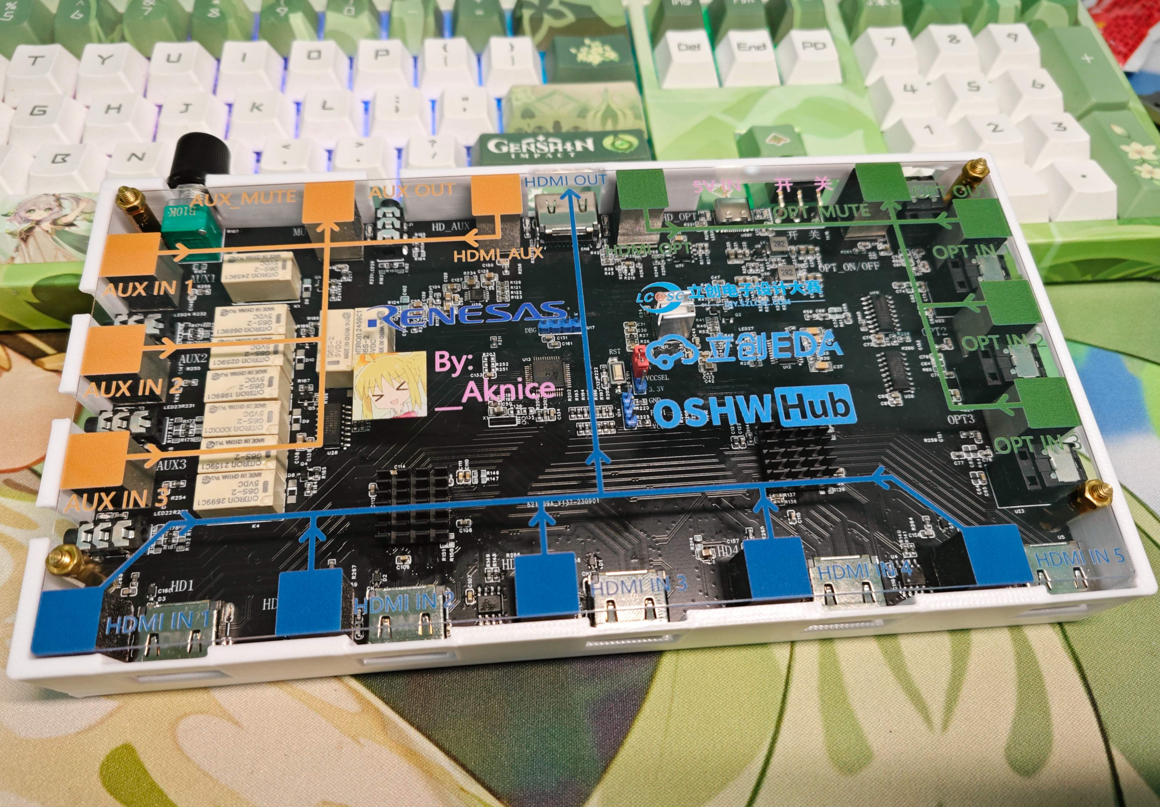
1. Introduction: This
audio/video switcher uses Renesas chips for main control and touch detection, two MS9601s for HDMI 5-to-1 switching, an MS9331 for HDMI audio decoding, relays for analog audio switching, and a CH444G for S/PDIF switching

. 2. Actual Usage:
I have many HDMI and audio devices, including various Raspberry Pis, Orange Pis, desktops, laptops, game consoles, disc players, and cassette players.
However, I only have one monitor and one speaker. Therefore, I wanted to share these peripherals among these devices, which is where the switcher comes in.
There are many
HDMI switchers on the market: HDMI

audio decoders,

audio switchers, and

fiber optic switchers.

However, they are expensive, and each component is separate, making wiring cumbersome.
Although the price wasn't their problem, it was mine—I simply couldn't afford it!
But I could do it myself.

So, this is what the back of my computer looked like before—a complete mess.
This was a compilation of several projects, so there were a lot of cables.

With this integrated solution, I could remove and

replace everything. Afterward
, there were far fewer cables, and it looked much better than before, but it was still messy (sad).

So, I placed the switcher under the monitor, so I could just take it out when switching.

3. Block Diagram
The main block diagram is as follows. Note the power supply usage. The analog audio and optical fiber light indicators and controls use the same set of control signals. The layout

can basically refer to the block diagram.

4. Circuit Schematic
4.1 Controlling HDMI Signals
According to the MS9601 datasheet, the RX HPD signal can be sent to the corresponding port to switch the corresponding HDMI to that port.

Therefore, the control is very simple; you only need to control the HPD high and low levels.
Often, after the input device detects HPD, it will output a differential video signal.
First, we need to understand the working principle of HPD (hot-swappable):
HDMI has input and output terminals. The input is the monitor, and here we have HDMI 3 inputs. The output is the computer graphics card, and here we have HDMI 1 output.
When an output device is connected to an input device, the input device will output the video signal at high speed via the HPD signal line. Once the input is ready, the input device will begin EDID communication and video signal transmission.
Therefore, controlling HPD controls the input device, specifically whether the MS9601 initiates EDID communication with the output device.

HDMIEN_MID is an intermediate signal relay, controlling the switching between input from chip 2 and output from chip 1. When using HDMI1, HDMI2, and HDMI3, HDMIEN_MID needs to be pulled high to switch inputs to chip 1.
4.2 HDMI Signal Flow
: As shown in the block diagram, HDMI signals 1, 2, and 3 are input to the preceding chip of the MS9601. This chip then outputs to the input of a subsequent chip, and HDMI signals 4 and 5 also enter the subsequent chip.
The signal input and output between these two chips can be directly connected.

The output of the latter chip is then fed to the MS9331. The 9331 detects and directly uses 5V for the HDMI DET

HPD input signal, retaining the original input method of two 3904s. A 47K

4.3 indicator light is pulled up by the IIC
. Due to the limited port resources of the RA chip, it is impossible to allocate four I/O ports for OPT and AUX control. However, two I/O ports can output four states, which can still be used for switching and indication. For indication, a 74LS139 logic chip
can be OPT as an example:
A:0 B:0 -> OPT1 A:1 B:0 -> OPT2 A:0 B:1 -> OPT3 A:1 B:1 -> OPT4
The same applies to AUX.

4.4 AUX
analog audio is directly switched using a relay, a pure physical switching, ensuring the original analog audio quality without going through a digital switcher!
The analog audio side has a separate ground wire, which is not connected to the entire GND circuit, resulting in the purest original sound quality (very Hi-Fi).
Therefore, an additional GND switching relay is needed.

The AUX input, besides indicating, also needs to control the relay's enable function, hence the output EN1234, connected to the relay's transistor control.

5.
LAYOUT: The most technically demanding part of this project is the layout. Due to the use of a large 20x10 PCB, a double-sided board is used to reduce manufacturing costs, but this increases the wiring difficulty. Therefore, pre-planning various rules is essential.
This project uses HDMI high-speed signals, requiring high-precision wiring. However, the interaction uses touch, and touch signals also have high wiring requirements. The analog audio switching signals also have high wiring requirements. The combination of these three factors significantly increases the difficulty.
5.1 Safety Spacing
Settings: Touch safety spacing

. 5.2 Copper Pour Spacing
Settings: Copper pour spacing for touch and HDMI. It is recommended to set a larger spacing


for touch. Set corresponding rules for both HDMI and touch signal networks.

5.3 Impedance Matching:
HDMI should be routed with 100 ohms impedance matching.


5.4 Layout:
I frequently design products with touch interfaces in my work, so I have some experience with touch layouts. Please feel free to correct any errors.
The overall layout is as follows. Actually, I personally feel that the ground plane is quite poor. A four-layer board would be much better.

I often use this plug-in HDMI connector. It is very easy to solder. Previously, I used surface mount connectors, which had many cold solder joints. This one is good, but there are two signal lines at the back, so the routing is more convoluted and will cross.

HDMI differential parameter settings are as follows. It is recommended to set the spacing to 3 times the line width, i.e., three times 9.2, but this is not set here, and the default 15mil is used. When

controlling the differential error to within 5mil,

HDMI signals and touch signals should cross vertically
and avoid crossing as much as possible.

Touch traces should be as thin as possible; avoid making them too thick. Double-sided boards can currently achieve 4mil traces, but to balance yield and minimum trace width, I've used 6mil traces here.

Minimize touch vias, ideally to 1 or 0. Keep via diameters as small as possible; for double-sided boards, the minimum outer diameter is 0.5mm and the inner diameter is 0.3mm.
Some touch lines here use two vias due to layout limitations.

Teardrop-shaped touch signals are generally avoided, but I'm too lazy to delete them all, and to maintain PCB yield, I've retained them.

Copper plating around the touch pads increases interference immunity, but be careful not to place them too close together. Also, it's not recommended to place surrounding components near the pads. Here, we've compromised by placing them next to the pads for the sake of the indicator lights.
Make the touch pads as large as possible to increase sensitivity and interference immunity. Whether or not to plating

copper on the back of the pads depends mainly on the panel thickness.
Thicker panels don't need copper plating, while thinner panels require a grid of copper. This grid copper shouldn't be placed in the exact center of the pad; it needs to be placed around it (this might be a bit abstract; we'll demonstrate with examples later).

Note that the touch pads are open; not having them open will affect sensitivity.

Pay attention to the routing of touch resistors and capacitors.

Incorrect examples:

Avoid parallel routing of touch and high-speed signals. I've separated them slightly here, but unless absolutely necessary, parallel routing is still not recommended.

Avoid placing touch sensors under relays, inductors, or other components that cause magnetic interference; keep them as far away as possible.


There are quite a few people playing with touch on open-source platforms. Actually, there's an element of mystery involved in touch; many people find it difficult to adjust, but it's not that hard.
There are still many intricacies I haven't covered here, so I'll stop here. I'll delve deeper into the various rules when I have more experience with touch engineering. Later, I'll compile a touch design guide for those interested in touch technology.
6. Chip Purchase
6.1
MS9331 The MS9331 uses IIC control. As usual, datasheets and register tables for MS chips are unavailable. However, like previous MS chips, there are compatible MS8005 ICs available online, so you can use a ready-made one without programming.
https://item.taobao.com/item.htm?spm=a1z09.2.0.0.5f152e8dYHRKFr&id=691533336994&_u=hqavhl8b1f1

6.2 MS9601 Chip
This store has a decent supply of chips, but there's a minimum purchase quantity. Buying just one will require additional shipping fees, so I recommend buying three or more.

Link: https://item.taobao.com/item.htm?spm=a230r.1.14.18.44ce4a89OI2g1U&id=664865791026&ns=1&abbucket=1#detail
Specifications: 24C16 programming
7. Shell Design
The shell is designed using SOLIDWORKS.


Screws:

Type
Parameter
Quantity
Single-pass hexagonal copper post
M3X6+6
4
Single-pass hexagonal copper post
M3X14+6
4
Copper hexagonal nuts
M3
4
304 Phillips head machine screws
CM3X6
4
8. Panel Drawing:
While drawing the outer casing in the previous step, draw the panel casing as well. Then export the DXF file and import it into LCSC EDA for panel drawing.

The touch pads need to be aligned for accurate drawing.
Select "Export Top Layer Solder Paste

," keep the touch positions, and delete other unused pads,

board outlines, and SW drawings. Align the imported elements and draw accordingly.

I personally recommend 1mm; I tried 2mm, and the touch sensitivity was slightly lower, but it was still recognizable.

9. Assembly:
First, install the conductive cotton,

then the two copper pillars.

After placing the panel down, tighten the nuts and

install it into the casing. First, install the upper right corner, then insert the toggle switch, then install the lower left corner. Next, tighten

the screws on the back, and

finally install the volume knob

. 10. Renesas MCU Software:
This time, I used the R7FA2E1A72DFL.
MCU resources are limited, basically utilizing all I/O ports.
10.1 I/O Configuration:
This project is relatively simple, without communication functions; it's mostly I/O control. Therefore, no special

debugging ports were reserved. Touch debugging uses

UART, which wasn't actually used. Later, it can be reserved for PC control of the

touch ports. Most ports are used

, with some control I/Os for output but no input.

10.2 Touch Logic:
It's very simple; pressing a button changes the corresponding I/O. There's no difficulty


. One touch function is that pressing a button lights up the P407's LED, and releasing it turns it off.

The default interface switching level is preset during initialization.

11. Touch Debugging
Notes: Touch sensitivity debugging is very limited by assembly. First, reassemble the panel and casing, and then perform touch sensitivity debugging!
It's recommended to do this step simultaneously with the previous code writing.
Touch debugging requires the conductive cotton to be properly assembled. I used 10x10x15 conductive cotton.
Note: When purchasing, pay attention to the description or ask the seller if the adhesive on the conductive cotton is conductive! This is very important. Some adhesives are not conductive.


After installing the conductive cotton, install the copper pillars provided in the outer casing. Because I chose 15mm high conductive cotton, I used 14mm high copper pillars, which pressed down just right. I do not recommend using 13mm pillars as they will not press down.

The conductive cotton just touches the panel.

Once everything is assembled, you can proceed with the assembly. Note that you should lead the debugging wires to the simulator
and then use the E2's CapTouch for debugging. Follow the instructions step by step to
set the corresponding touch key positions

. The touch resistor needs to correspond to the surface mount resistor. Here, I did not use the default 560 ohms but replaced it with 470 ohms. The program is also set to 470 ohms.
The touch debugging is as follows: after exceeding the threshold for a while, the button will be triggered, and the desired action can be executed.

12. Summary:
The technical content of this project mainly lies in the touch wiring and interaction, including the touch layout rules and the compatibility of touch with high-speed signals.
The debugging process of this project is different from ordinary projects. Due to the addition of touch, the touch sensitivity is very limited by the structural assembly. Therefore, debugging can only be carried out after the assembly is complete.
The highlight of this project also lies in the ingenious combination of structural and electronic technologies, such as the conductive cotton used for the interaction between the touch pads and the panel.
On the software side, the main focus is on the debugging and coordination after the touch panel is installed.
This project was almost perfectly executed using JLCPCB's supporting infrastructure, including EDA design, PCB manufacturing, online sourcing, SMT, panel design, and 3D printing by 3Dmonkey. It also benefited from Renesas' support and the e2 software's optimized touch compatibility.
The main purpose of this project was to address my increasing number of device switching, frequent HDMI cable unplugging and replugging, and the growing number of cables at the back of my computer!
Choose 5V for the MCU power supply; do not use 3.3V.

For high-speed display devices, it is recommended to connect to HDMI 5 and 4, prioritizing HDMI 5 and 4 inputs. This avoids the need for a switching chip and reduces heat generation. It
is recommended to add heatsinks to the MS9601 and MS9331 chips, as they generate significant heat.

It's a pity that USB switching wasn't included in this KVM switch, as adding a board would cost over 100 RMB. Therefore, I'm currently using a USB 3.0 switch I made last year.

This year, I will make a KVM switch integrating various components, including a remote control (which requires standing up and manually pressing buttons, which I find quite inconvenient).
This project mainly focuses on cost accounting. The casing was self-printed, so no estimate was made. The total cost is approximately 130 RMB.
Material
prices :
PCB board
60x5 pieces, 12 RMB per piece;
MS9601
10 RMB x 2 = 20 RMB;
MS9331
12 RMB x 1;
MCU ...
8 yuan x 1
relay,
2 yuan x 9 = 18 yuan,
fiber optic receiver,
3 yuan x 3 = 9 yuan,
conductive cotton,
10 yuan,
panel
from LCSC, 22 yuan (shipping not included)
, other peripherals, resistors, capacitors, etc.
, approximately 15 yuan.
13. Competition certification logo.


RA Switch Housing 3D Panel DXF.7z
[e2] RA Switcher KVM Code.zip
Competition Certification Logo.mp4
Touch test.mp4
HDMI Switching and Audio Test.mp4
AUX switching demonstration.mp4
Fiber optic switching demonstration.mp4
PDF_#8th LCSC Electronics Design Contest# Audio/Video KVM Switch (Fiber Optic, Analog Audio, HDMI).zip
Altium_#8th LCSC Electronics Design Contest# Audio/Video KVM Switch (Fiber Optic, Analog Audio, HDMI).zip
PADS_#8th LCSC Electronics Design Contest# Audio/Video KVM Switch (Fiber Optic, Analog Audio, HDMI).zip
BOM_#8th LCSC Electronics Design Contest# Audio/Video KVM Switch Fiber Optic, Analog Audio, HDMI.xlsx
91052
Prototype Multifunctional Observation Instrument [Wasteland Heavy Industry]
Design a multi-functional observation device with a head-up display (HUD). Its functions include short-range distance measurement (within 2 meters), temperature and humidity measurement, and compass orientation. These parameters can be projected onto the HUD. The device can meet the environmental detection needs of wargames, outdoor exploration, and wilderness search and rescue.
Foreword
by Old Popsicle: Please note that this device is difficult to build and has high material costs.

This particular device is primarily for functional verification and entertainment, and mass production is not a consideration. Please be aware that
I will likely continue to improve the design of each part; at least the next version will look much better.
DEMO.zip
Shell_V2.zip
Function demonstration.mp4
PDF_Prototype Multifunctional Observation Instrument [Wasteland Heavy Industry].zip
Altium Prototype Multifunctional Observation Instrument [Wasteland Heavy Industry].zip
PADS Prototype Multifunctional Observation Instrument [Wasteland Heavy Industry].zip
BOM_Prototype Multifunctional Observation Instrument [Wasteland Heavy Industry].xlsx
91053
[Junior High School Graduation Project] Electromagnetic Railgun
The copper pillar structure charging buffer photoelectric control self-discharge circuit requires no flying wires or MCU;
all circuits are integrated onto a single PCB, eliminating the need for wires and simplifying manufacturing.
With the rapid development of science and technology, China's electromagnetic railgun technology has long surpassed that of many developed countries, taking the lead in the world. Now, sharing in the benefits of the country's rapid development, we can easily build our own electromagnetic railguns at home at low cost.
**Disclaimer:
** A sound legal environment requires everyone's joint efforts to maintain; please remember and strictly abide by relevant national laws!
This project strictly adheres to national standards.
It was independently developed and is open-source by the author. Please do not reproduce it without attribution, and please do not use it for commercial purposes without the author's permission (although it seems unlikely anyone would need it, but what if?). You can contact the author via WeChat: WZ1476001 (apologies for not being able to reply promptly due to the upcoming high school graduation season and only being able to go home once a month).
This circuit contains high voltage; please understand the circuit before using it carefully (do not attempt to build it without relevant electronics knowledge, as there are significant safety hazards).
Do not touch the two high-voltage contacts. It is recommended to use insulating heat-shrink film for side insulation and insulating silicone for the first and last high-voltage circuits. The author and platform are not responsible for any safety issues that arise.
Special thanks to:
Dad: Thank you Dad for generously sponsoring the 4 IGBTs!
JLCPCB: Thank you JLCPCB for providing convenient and practical development tools and a good open-source environment for domestic developers, as well as the twice-monthly free PCB prototyping.
Key component materials:
Capacitors: Two 450V 820uF aluminum electrolytic capacitors, 25mm*60mm in size
. Coil: 0.8mm wire diameter, 150 turns, overall height 28mm, outer diameter 20mm, inner diameter 8mm.
Electronic switch: Uses a high peak current automotive-grade IGBT, model AIKQ120N60CT (silkscreen: AK120DCT), peak current 480A. Please refer to the datasheet for specific parameters (AIKQ120N60CT_PDF_Datasheet_Specification Book - Semiconductor Chip (semiee.com)).

Please note that if you did not purchase a genuine IGBT from a professional platform, please do not apply excessive voltage, otherwise it will burn out. Thank you again to my father for sponsoring the four IGBTs!
Protection Diode: High-current fast recovery surface-mount diode RS5M, operating current 5A, corresponding to the through-hole model FR507. Surface-mount packaging is chosen for ease of soldering and a more elegant appearance.
Discharge Resistors: R8~R13 are six 2W power boost resistors in 2512 packages. When purchasing resistors, please be careful not to buy ordinary resistors with a success rate of 1W, otherwise it may burn out the resistor.
*All surface-mount components in this circuit use packages no smaller than 0805 to reduce the difficulty of hand soldering.
* The cost of the fourth-level component is around 200, which is very low. Interested students are welcome to try it.
*During the drawing, because some components did not have 3D models, I used renamed components with the same package as substitutes. When ordering components, please search for the model number yourself. Do not order directly according to the BOM file, otherwise it may lead to incorrect model numbers.
Key Network:
+12V: 12V control power network (I used a 3S lithium battery).
VCC: VCC-D1 voltage drop ≈ final capacitor charging voltage. VCC is the output of the boost module. It is recommended to connect VCC at the first stage (see [Copper Pillar Structure] for details). The preset VCC is 250V in the design, but it can be freely adjusted between 5V and 360V (360V is 0.8 * capacitor rated voltage, with the remaining 20% as a margin).
C_O: Meaning Capacitance_Out, which is the positive terminal of the capacitor and also the input of the coil.
L_-: The output of the coil.
GND: Common ground.
Copper pillar structure:
This electromagnetic gun uses a copper pillar energy transmission structure, with one M3 copper pillar connected to each of the four corners. Special thanks to the Bilibili UP master @-中中- for sharing this excellent energy transmission method. His video was very helpful and inspiring for me when I was in the second year of junior high school and just learned about electromagnetic guns. I highly recommend that interested students watch it (the specific video title is: [Hardcore & Record] I spent 5 years making 8 generations of electromagnetic guns!!!).
The copper pillar in the upper left corner is defined as the +12V power network and is directly connected to the positive
terminal of the 12V power supply. The copper pillar in the upper right corner is defined as CONNECT. When K1 on the circuit board connected to the high-voltage power supply is triggered, VCC will be connected to the CONNECT network of each stage of the circuit board through two NTC thermistors.
The two copper pillars at the bottom belong to the same network. GND.
The following is a detailed explanation of each part of the circuit to help students who are just beginning to learn about electronics understand
(including some detailed explanations).
[Capacitor Charging]
This circuit uses two NTC thermistors for current limiting to prevent contact sparks within the switch and extend its lifespan. However, since a 2A microswitch is used, it's also possible to omit the NTC thermistors and directly short-circuit their contacts.
When K1 on the high-voltage power supply circuit board is triggered, VCC will connect to the CONNECT network of each stage of the circuit board via the two NTC thermistors. Therefore, in the [Capacitor Charging] circuit, only K1, R1, and R2 need to be installed on the circuit board connected to the high-voltage power supply (VCC). It's recommended to install them on the first stage; if installed on a later stage, K1 may be obstructed, making it inconvenient to use.

[Voltage Indication]
Two S8050 transistors are used in the two high-voltage indicator circuits on the left connected to capacitors to avoid excessive power consumption caused by direct capacitor connection and to prevent the LED from ignoring voltage fluctuations. The indicator light is not lit when the voltage is low and too bright when the voltage is high
because the indicator circuit is directly connected to the two ends of the capacitor. Therefore, it can also be used as a discharge indicator. When the voltage is greater than about 10V, the red light is on, indicating that the capacitor is charging or the voltage has not been fully discharged. When the voltage is greater than about 220V, the green light is on, indicating that the preset voltage of 250V has been reached (the voltage is preset to 250V in the circuit design, but it can actually be higher or lower). An external 500V LED voltmeter can also be connected as a voltage indicator.
The blue indicator light on the right is used to indicate that the 12V power supply is normal.

[Capacitor Discharge]
The purpose of this part of the circuit is to prevent the high voltage stored in the capacitor from injuring people
when the capacitor voltage is not fully discharged but is not emitting. When the capacitor voltage is 250V, after the discharge switch is turned on, the voltage across the capacitor drops to a safe voltage for the human body after 25 seconds. After the switch is turned on for 40 seconds, the capacitor voltage drops to about 10V.

[Photoelectric Signal]
LED4 is an infrared emitter, and LED5 is an infrared receiver. When LED5 receives infrared light, its resistance is close to 0, and the voltage between the base and emitter of Q3 is too low, causing it to cut off. PC817 does not trigger, and the voltage in the Q6_Control network is 0V at this time. When the shell blocks the infrared light, the resistance of LED5 rises sharply. At this time, the base of Q3 is at a high potential, Q3 conducts, LED6 is lit as an indicator light, and the internal LED of PC817 also lights up simultaneously. Pin 43 conducts, and the voltage in the Q6_Control network is close to 12V.

[Coil discharge]
When the Q6_Control network is high, Q4 does not conduct and discharge because the BE stage is high. ZD2 controls the voltage at 10V, so there will be a 10V voltage between the GE stages of Q6. When the Q6_Control network is low, the base stage of Q4 is at a low potential, the CE stage conducts, and the voltage between the GE stages of Q6 is quickly discharged. Because there is a very small voltage drop between the CE stages of Q4, the voltage between the GE stages of Q6 cannot be completely discharged. Therefore, a 10K resistor R19 is added to ensure complete discharge.

PCB layout:
The largest core components—capacitors, coils, and IGBTs—as well as two relatively large connectors are placed on the back of the PCB. The larger K1 on the front only needs to be installed in the first stage (the first stage is recommended), which makes it easier to build multiple stages. The
upper part is the control signal generation part of the circuit.
The upper right part is the charging control circuit. The lower part
is... The discharge circuit uses six 2W boost resistors. At 250V, the actual operating power is slightly over 11W.
The left side shows the voltage monitoring circuit.
PCB dimensions: 5.55cm * 5.4cm.

Operation
:
First, switch the discharge switch to the OFF position. Then press K1 to charge the capacitor. When the voltage reaches the preset voltage, release K1 and switch the launch switch to the ON position. If a projectile is blocking the photoelectric switch, it will fire immediately. Alternatively, you can turn on the launch switch first and then load a projectile. When the projectile blocks the photoelectric switch, it will fire automatically.
When not in use:
First, switch the launch switch to the OFF position. Then, switch the discharge switch to the ON position to discharge the capacitor. When the capacitor voltage is 250V, it will discharge for about 25 seconds to drop to a safe voltage for the human body, and for about 40 seconds to drop to 10V. Do not touch the capacitor terminals before the voltage drops below a safe voltage for the human body.
That
's the final product. What do you think?
(This dog ran over on its own.


For speed measurement,
it's suggested to add a blank PCB without a power system after the final stage of the electromagnetic cannon. One reason is for a neater and more aesthetically pleasing design. Also, if you have an oscilloscope, you can use this PCB for speed measurement. The specific operation is as follows:
To achieve speed measurement using the last board, we need to solder the [photoelectric signal] circuit on this last PCB.

The author left two pads labeled [T+] and [T-] on the left side of this circuit. When a shell blocks the infrared receiver from receiving infrared light, the emitter of Q3 will be at a high level, with the voltage being the diode voltage drop at the PC817 control terminal plus the voltage drop of LED6, approximately 4V~4.5V. These two points are directly connected to the positive terminal of LED6 and pin 2 of PC817.
Modulating the oscilloscope to DC pulse detection mode allows you to measure the duration of this high level, which is the time it takes for the shell to travel the distance of the shell's length (I used a 20mm shell). Then you can...) The projectile's velocity can be calculated using the middle school equation v=s/t. For example,
if the projectile is 20mm long (0.02m) and the high-level signal lasts 10ms (0.01s), then the projectile's velocity would be 0.02m/0.01s = 2m/s.
However, this method has some errors and is slightly cumbersome. Those with the means can directly purchase an electromagnetic railgun velocity measurement module; this is merely a more economical reference solution.
Regarding the next generation
, since I'm about to enter high school, I may not have much time to complete its development in the next three years.
However, I've already envisioned the framework for the next two generations. Therefore, the next generation should be released by me after graduating high school and having some free time. Of course, if everyone supports this project, it might be released by me during my three years of high school, but I hope this article can be helpful to those just starting out in electronics. The next generation, the second generation, the third generation... will be developed by everyone who loves learning. The current generation of open source
still has many areas for improvement. Here are my thoughts briefly for those interested:
The structure still uses a four-copper-pillar design, but the first stage is now a ZVS power board/control board. The +12V copper pillar is replaced with a signal copper pillar. The subsequent stages only receive +12V power after the start switch on the first-stage power board is turned on. The switch for the subsequent stages
is removed; it is in the on state when it receives 12V, eliminating the need to turn on each transmitter switch individually.
Consider merging the CONNECT network directly with the C+ network. This would allow you to draw only the voltage indicator circuit on the first-stage power board
, eliminating unnecessary coil discharge circuits. Just make sure not to charge it when not in use, which would allow for a smaller size.
Also, replace the two capacitors with a single, larger-capacity flash capacitor. The specific placement is not yet well-planned.
It would be best to further optimize the capacitor charging limit circuit on the first stage.
Change the IGBT from through-hole to surface-mount, instead of blindly following trends. I need high current parameters for IGBTs. I'm looking for high-performance, cost-effective, and suitable
options. After modifications, the entire circuit only has a capacitor charging limit circuit, voltage indicator circuit, and two control switches in the first stage. The subsequent stage circuits are much simpler and smaller.
Regarding safety, I haven't found a safer or more convenient method than using insulating heat-shrink film for side insulation and insulating silicone for insulation of the first and last high-voltage lines. If you have better ideas, please share them in the comments section.
If you are interested in electromagnetic guns or electronic circuits but lack electronics knowledge, I recommend watching the videos of a teacher on Bilibili, 【多多百科】. This teacher was my introductory teacher for electromagnetic guns and electronics. He explains things while demonstrating, and his explanations are easy to understand. Many of his videos were very helpful for me when I first started learning about electronics.
Finally, I strongly suggest using PVC insulating heat-shrink film for side insulation and insulating silicone for insulation of the first and last high-voltage lines to eliminate safety hazards. Safety first!!!
*Only version V3.0 is correct in the circuit diagrams below. The other versions are discarded products from recent brainstorming sessions, and their PCB structure and layout have some issues. Therefore, not much time was spent revising the circuits. There are many errors in the circuit diagrams and PCB layouts. Interested students can take a look.
PDF_[Junior High School Graduation Project] Electromagnetic Gun.zip
Altium_[Junior High School Graduation Project] Electromagnetic Gun.zip
PADS_[Junior High School Graduation Project] Electromagnetic Gun.zip
BOM_[Junior High School Graduation Project] Electromagnetic Gun.xlsx
91054
ESP32 Universal Remote
This project uses the ESP32-S3 to create a universal remote control, serving as a general control solution for various RC models and robots.
It can also connect to a computer via Bluetooth for gaming, or allow users to play custom-written games directly on the remote control.
Finished Product Showcase:
DIY Universal Remote Control - Bilibili

Project Description:
When playing with various RC models, robots, or other toys, each has its own remote control, which can be quite messy. Therefore, I wanted to create a universal, multi-functional remote control.
It can not only control numerous devices but also connect to a computer via Bluetooth to play AAA games as a Bluetooth gamepad. It can even be used to create and play small games.
Achieving the elegance of "one control in hand, the world at my fingertips!"
Project Features
: 1. This remote control is based on the ESP32-S3 chip. For ease of construction, a development board with a screen was used. The 1.91-inch screen boasts a high resolution of 240*536, providing excellent display quality.
2. The remote control features 4 standard buttons, 4 toggle switches, 2 potentiometer knobs, 2 high-precision RC joysticks, 8 function buttons, 2 onboard buttons, and 1 MPU-6050 electronic gyroscope.
3. The communication module uses a 20dBm nRF24L01 module, paired with a 3dBi gain antenna, achieving a remote control distance of over 2000 meters.
4. Two 2600mAh high-capacity 18650 lithium batteries ensure long battery life for the remote control, and the development board integrates a charging and discharging module, eliminating battery anxiety.
Design Principle:
The remote control's working principle is simple: it continuously reads the status of each button and joystick, combines the button values and joystick analog values into a self-designed structure, and sends this data to the receiving end via the nRF24L01. The receiving end parses the data and responds accordingly.
Shell Design:
The shell design has three requirements:
1. Comfortable grip:
Numerous chamfers and rounded corners conform to the hand, preventing gripping and slippage.
2. Ease of manufacturing
: Irregularly shaped parts are separated into components, maximizing flat surfaces for subsequent 3D printing. Separate components also facilitate multi-color printing.
3. Aesthetics:
While meeting the first two points, strive for a visually appealing design, or add some unique features.

Production Process
: 1. First, purchase all components from the assembly list (detailed list in the attachment).

2. Solder the components onto the pre-made PCB (component list in the attachment)
and install the development board and battery onto the board. Connect the development board and PCB power supply through the central hole using a wire.

3. 3D print the outer shell and all buttons and knobs (printing files in the attachment; the outer shell includes a blank version).

4. Install the electronic components onto the outer shell (like putting an elephant in a refrigerator).

5. Finally, install the button caps and antenna; the remote control hardware is now complete.

The remote control test code
works by continuously polling all buttons and displaying their status on the screen.
Programming is based on the Arduino environment, using the TFT_eSPI graphics library; detailed code is in the attachment.
Actual Test Results:
You might wonder why the small screen is facing down in the test video below.
For details, please see the video: DIY Universal Remote Control_Bilibili_Bilibili
Updated September 27, 2023:
Menu System Structure -

First and Second Level Menu Preview -
First Level Menu:

Partial Second Level Menu:


Menu and Remote Control Effect Test.
I used a previous tracked chassis for testing, and the results were good.
See the Bilibili video for details.

Menu Source Code and Icons
: The complete source code and icons are attached.
This system will be improved periodically; please follow the Bilibili account 【黑黑黑科技】 or this project.
Controller Code.zip
Remote Control Case V2.zip
Create PCB files.zip
Hardware List.xlsx
Demo.mp4
icon.zip
Remote control system framework code.zip
PDF_ESP32 Universal Remote Control.zip
Altium_ESP32 Universal Remote Control.zip
PADS_ESP32 Universal Remote Control.zip
BOM_ESP32 Universal Remote Control.xlsx
91055
LoRaWAN multi-channel relay
This LoRaWAN four-channel relay is based on the E77 (ARM Cortex-M4 + LoRa) SoC wireless communication module. It supports wide voltage input, has two power interfaces, and adopts an optocoupler isolation scheme, making it suitable for applications in home, industrial, agricultural, and other scenarios requiring remote operation.
The current version 1.0V
test code has been uploaded as an attachment. Please leave a message at the bottom if you have any questions.
1.0 Update Log:
Added onboard electrical isolation.
Modified optocoupler isolation circuit.
Modified PCB size.
Added LoRa signal indicator.
Project Introduction :
Based on the E77 (ARM Cortex-M4 + LoRa) SoC wireless communication module, LoRaWAN four-channel relay. Supports wide voltage input, two power interfaces, and adopts an optocoupler isolation scheme, applicable to scenarios requiring remote operation such as home, industry, and agriculture.
Accompanying open-source project: E77 Ebyte LoRaWAN Development Board.
Project Functionality:
The main controller uses the E77 module from Ebyte. The E77-400M22S is based on ST's newly launched STM32WLE5CCU6 (ARM Cortex-M4 + LoRa) SoC wireless communication module, featuring long-range communication, low standby power consumption, strong anti-interference capability, rich interface resources, strong processing power, and small size. It is applicable to 433/470MHz band surface-mount LoRa wireless modules, using industrial-grade high-precision 32.768KHz and 32MHz crystal oscillators.
This product is a four-channel relay switch, supporting local button control or remote LoRa control. It uses four-channel optocouplers for high-voltage isolation and has double isolation treatment on the PCB.
The power supply section supports DC/AC 7-40V input and has built-in rectifier devices for power protection.
Onboard reserved programming pins facilitate debugging and program download.
Software Description
Most of the software code is provided in the attachment. Currently, the basic test code is tentatively uploaded
[ ] indicating incomplete
[x] indicating completed and uploaded attachment
code Progress:
[x] Basic code test
[ ] Point-to-point code test
[ ] Gateway linkage code test
Physical display Instructions


Precautions
When soldering, please pay attention to the soldering order to ensure the power supply is correct and not burn out the subsequent circuits! The soldering order should follow the principle of from shortest to smallest and from inside to outside.
Demo video.mp4
Keil.STM32WLxx_DFP.1.1.0.pack
LED_USART_TEST.zip
PDF_LoRaWAN Multi-Channel Relay.zip
Altium_LoRaWAN multi-channel relay.zip
PADS_LoRaWAN Multi-Channel Relay.zip
BOM_LoRaWAN Multi-channel Relay.xlsx
91056
Liangshan School Oscilloscope - Dual Channel
Dual-channel oscilloscope design based on Liangshan School
Project Analysis:
This project is based on the Liangshan School design of a dual-channel oscilloscope
to achieve the following functions:
1. Dual-channel acquisition ;
2. DAC waveform generation;
3. Dial button control;
4. Screen touch control.
Overall Hardware Block Diagram:

This project is based on an official case study, which is as follows: [Oscilloscope Expansion Board].
My work includes:
1. Drawing a dual-channel acquisition circuit based on the official single-channel acquisition circuit
; 2. Drawing a screen touch circuit to replace button operation;
3. Removing the tactile buttons and retaining the dial buttons;
4. Using screen touch + dial buttons to complete human-computer interaction;
5. Adding a power supply interface;
6. Designing the PCB based on the drawn schematic.
7. Solder and debug the oscilloscope.
8. Complete the dual-channel oscilloscope code
schematic design. Instructions:
1. AC/DC Coupling Circuit:
This project uses a relay to simultaneously control the AC/DC coupling of two ADC acquisition circuits. Switching the relay switch is achieved by changing the GPIO level.

2. Voltage Divider Circuit, Programmable Operational Amplifier Signal Processing Circuit, and Waveform Generator Output Voltage Follower Circuit:
These three circuits are all based on official examples and will not be explained further here. Please refer to the official documentation [Oscilloscope Expansion Board].


3. Power Supply Section:
The level conversion in the power supply section is based on official examples. I won't go into too much detail here
. Based on the official documentation, I added a power supply interface because when using the official oscilloscope extension version, the power supply interface interfered with the waveform acquisition and output channels, preventing normal operation. In this project, after modifying it to use the waveform acquisition channel, one channel became unusable. Therefore, I added a power supply interface to ensure stable operation of both channels.

Also, please note that the oscilloscope uses a +2.5V ADC reference, but the Liangshanpai version uses a 3.3V reference. Therefore, the A3.3V and AGND 0Ω resistors in the Liangshanpai version need to be removed. The official documentation specifically notes the following:

4. Screen Circuit:
This project uses a 2.4-inch SPI screen. A touch circuit is added to the official display circuit to achieve touch interaction on the oscilloscope. Both display and touch use SPI communication.

5. Button Circuit:
This project uses two DIP switches and screen touch to achieve human-computer interaction on the oscilloscope.

PCB Design Description:
This project requires the placement of many components, so I lengthened the board during the design process. The width is consistent with the core board of Liangshanpai, as shown in the figure below.

The PCB layout is relatively compact, which significantly impacts routing. Therefore, this project ultimately adopted a 4-layer board design. Inner layer 1 is used as an analog ground plane. Inner layer 2 is only connected to some power and signal lines due to concerns about interference with analog signals (this is my first time drawing this, and I'm not sure if it will cause interference. If any experts can see this and explain the relevant knowledge, that would be excellent; please don't criticize).
In this project, two ADC detection probes are brought out, along with waveform generation test points and analog ground test points. The test loop is used for the waveform generation test point and the simulated ground test point, which facilitates the connection and testing of the oscilloscope probe .

Also, the component layout is relatively dense, making soldering slightly more troublesome.
Software instructions:
1. Initialization of dual-channel ADC
The two ADCs are PA1-ADC0CH1 and PF7-ADC2CH5. The acquisition idea is: the timer triggers ADC acquisition, DMA automatically stores the data, and when the data acquisition is halfway completed or completed, the DMA interrupt is triggered, and the acquired data is displayed in waveform form
in the ADC initialization function. PA1 uses the same pin as the official example and does not need to be modified. Only the PF7 part needs to be added.

Acquisition interrupt function of ADC2CH5

2. AC/DC switching and sampling rate switching control

3. Implementation of microsecond delay function
First, modify the systick.c function and modify the value of the systick clock reload register. The original value is system clock/1000. In this case, the practical interval of each interrupt entry is 1ms, so the original file only has the millisecond delay function. Modifying this value to system clock/1000000 changes the interrupt time to 1µs. Simultaneously, the original millisecond delay function is modified, thus completing the microsecond delay function implementation.

4. Touch Function Porting:
The touch chip used in this project is XPT2046. Screen vendors provide touch functions for XPT2046, but these are functions applied to ST chips and require GD porting.
The provided touch routines use software SPI, so this project also uses software SPI. The microsecond function implementation in the previous step mainly applies to the touch software SPI communication.
Due to batch differences and other reasons, the default calibration parameter values of the touchscreen may cause inaccurate touch recognition. It is recommended to calibrate before use; it is not recommended to directly use fixed default cali


 京公网安备 11010802033920号

 500-107Z169RSNB606


