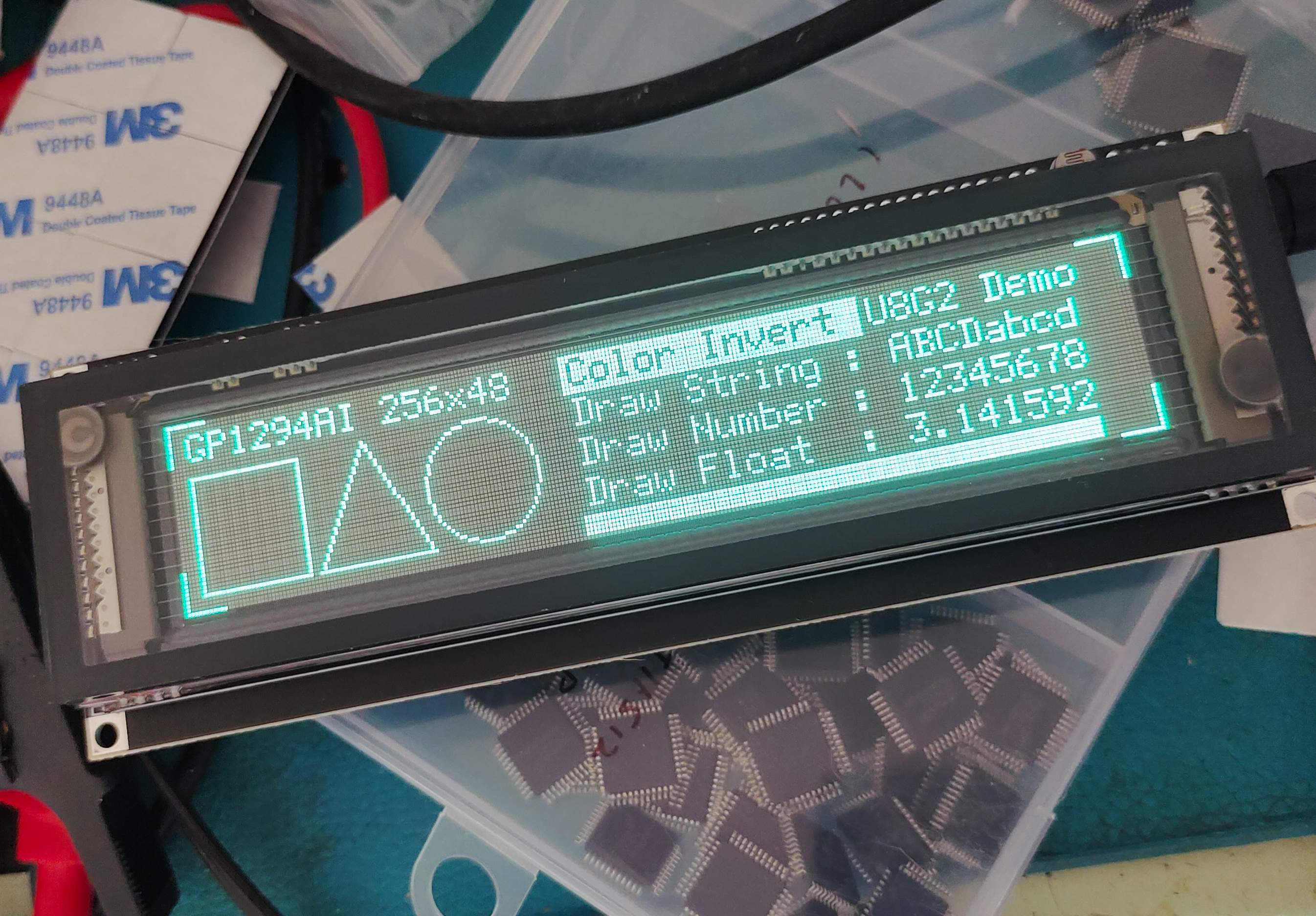
The EEI TECHNOLOGY 05P-FLUORITE UNL-200AP-B general-purpose VFD display module
features a wide voltage input range of 4.5-24V.
It adapts to 3.3V/5V levels (compatible with mainstream microcontrollers such as 51 and STM32).
An improved power supply and filament drive scheme eliminates feedback and increases efficiency.
The VFD screen has a built-in timing controller, effectively preventing screen burn-in due to improper use.
It offers 1024 adjustable brightness levels.
Maximum power consumption is approximately 3W (full LED illumination, 1024 brightness levels, 5V input).
Built-in dynamic scanning logic and RAM allow for display completion simply by sending instructions to the screen.
A reserved space for the main control board is provided on the PCB, effectively utilizing available space.
An audio input interface is provided for audio applications.
An onboard photoresistor, in conjunction with a microcontroller, enables automatic brightness adjustment.
TYPEC and DC005 power interfaces are available, compatible with various power supplies.
Copyright Notice:
This project and product specifications are copyrighted by EEI TECHNOLOGY Electronic Studio.
This project is licensed under the CC-BY-NC-SA (Creative Commons Attribution-NonCommercial-ShareAlike) license and unauthorized derivative works are prohibited (creating new projects by taking parts of the original project or modifying it is called a "derivative"). Even with authorization, the project must be shared in the same way before any derivative work can be done (the original author's name and source must be credited). Disregarding the open-source license and engaging in commercial activities will be pursued and severely punished by our studio! Please consciously abide by the open-source license and work together to maintain the open-source environment.
This project is for DIY and learning purposes only. It is prohibited to use this project for any commercial activities (selling, distributing, or copying for profit), including but not limited to the above three points.
Uploading the product specification sheet to other platforms, such as Baidu Wenku or CSDN, is prohibited.
To prevent individual vendors from speculating on the display screens, I have controlled the display screens for this project and are selling them at normal prices. Thank you for your understanding!
Note:
The driver board has high voltage; please handle with extreme caution.
This studio has completed the adaptation of the U8G2 library, providing the Arduino U8G2 library and a C language version
of the U8G2 project (STM32CubeIDE). Due to my limited programming skills, I am unable to develop other drivers; please develop them yourself if needed.
U8G2 project pinout: PA5 SCK, PA7 SDA, PA1 CS, PA3 RESET.
Datasheet link (extraction code: n6ix ).
Related purchase links:
VFD display
GP1294 display module board, front

panel, back panel,

display effect images,

product specification sheet (partial).


PDF_GP1294AI 256x48 VFD Display Module (UNL-200AP-C)_Pro.zip
Altium_GP1294AI 256x48 VFD Display Module (UNL-200AP-C)_Pro.zip
PADS_GP1294AI 256x48 VFD Display Module (UNL-200AP-C)_Pro.zip
BOM_GP1294AI 256x48 VFD Display Module (UNL-200AP-C)_Pro.xlsx
91063
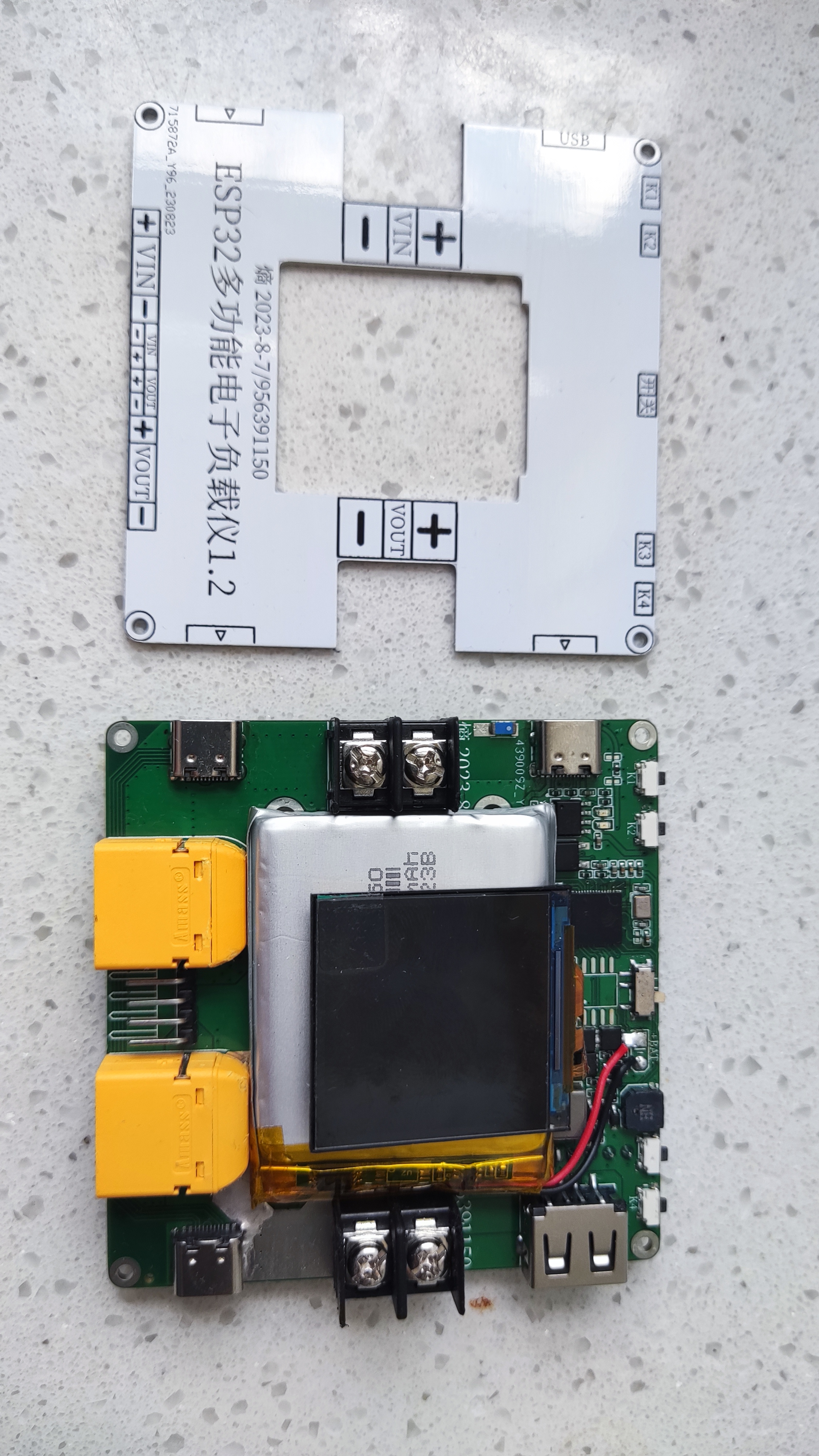
ESP32 CNC Electronic Load Unit
The ESP32 is a multi-functional, mini, portable DC digitally controlled electronic load and power meter powered by a built-in lithium battery.
Project Description:
The ESP32 Multifunctional CNC Electronic Load Tester is a portable DC CNC electronic load tester and power meter powered by a built-in lithium battery. It features multiple interfaces, supporting CNC constant current (CC), constant current (CV), constant voltage (CR) , constant resistance (CP), constant power discharge (CP), and real-time measurement and display of parameters such as current, voltage, power, and temperature
. Function Overview
: 1. USB TYPE-C interface supports program download and device power supply . 2. Input Ports: TYPE-C + XT60 + 2P gate terminal block + 2P header. 3. Output Ports: TYPE-C + TYPE-A + XT60 + 2P gate terminal block + 2P header. 4. ST7789V 1.54-inch 240*240 pixel color LCD display shows various parameters; display direction and brightness are adjustable. 5. One toggle switch controls battery power supply; four microswitches are used for mode switching and parameter setting. 6. Input Voltage: 0~50V; Input Current: 0~20.2A; Maximum thermal design power in electronic load mode: 200W. 7. 8. Real-time power transistor NTC temperature measurement protection and display with buzzer prompts. 9. Dual power supply from lithium battery and USB: Automatically switches to USB power and charges the lithium battery when USB is plugged in. 10. Features reverse connection, overvoltage, overcurrent, overtemperature, and overpower protection, as well as threshold settings and parameter saving after power failure. Open source license : This project is licensed under the "CC BY-SA 4.0" license. Please do not use it for commercial purposes. When reprinting, please include the original source link and this statement. Project Attributes : 1. This project is being publicly released for the first time and has not won any awards in other competitions. It is an original open-source project by Negative Entropy Birth Light (CC BY-SA 4.0). 2. Gitee repository link: https://gitee.com/arduino2021/ESP32-E-Load.git 3. Project Progress (August 29, 2023): 1. June 2023: Completed schematic and PCB design, prototyping, verification functions, bug finding, and started software development for ESP32 Multifunctional CNC Electronic Loader 1.0. 2. July 2023: Completed schematic and PCB design, prototyping, verification functions, and bug fixing for ESP32 Multifunctional CNC Electronic Loader 1.1, and started software development. 3. August 2023: Completed schematic and PCB design, prototyping, verification functions, bug fixing, and software improvement for ESP32 Multifunctional CNC Electronic Loader 1.2. 4. The project has undergone three iterations, costing over 600 RMB for PCB prototyping and component purchases. After more than three months of time and effort, the final design principles are as follows: 1. This project uses an ESP32-S3FN8 as the main controller, and uses an INA226 to collect voltage and current parameters in real time to control the output reference voltage of the MCP4726 DAC chip. 2. A constant current operational amplifier compares the DAC reference voltage with the voltage divider of the current sampling overcurrent resistor to control the VGS voltage of the power NMOS, thereby controlling the current flowing through it to achieve constant current control. 3. CC constant current control controls the current flowing through the power NMOS by controlling the output reference voltage of the MCP4726 DAC. 4. CP constant power control uses the formula U*I=W, which can be calculated by software to convert W/U = I into constant current control, thus achieving constant power control. 5. CR constant resistance control uses the formula U/R =I, which can be calculated by software to convert the current value into constant current control, thus achieving constant resistance control . 6. CV constant voltage control uses the ESP32-S3FN8 as the main controller because a general power supply is not an ideal voltage source and has internal resistance, so it cannot output an infinite current. Therefore, it can lower the voltage by consuming current to achieve constant voltage control. 7. Small current measurement is performed using an ESP32-S3FN8. The ADC acquires current information in the μA range by dividing the current through a 10R sampling resistor after amplification by a precision operational amplifier. Functional modes and buttons: 1. Electronic Load Mode: Long press K4 to switch between CC, CV, CR, and CP modes and set the time-limited operation time and cutoff voltage. Short press to select the parameter bit. Short press K1 or K2 to set the parameters for the corresponding mode. Short press K3 to control whether to run. 2. Power Measurement Mode: Automatically measures the input-output voltage, current, and power and plots the curve. Short press K3 to control the NMOS switch. Long press K4 to clear the mode's operation time and accumulated charge to 0 and restart accumulation. 3. Calibration Setting Mode: Long press K4 to switch between different calibration setting parameters. Short press K4 to select the parameter bit. Short press K1 or K2 to subtract or increase the parameter. Short press K3 to set or save the parameter. Default settings can be restored. 4. Button Functions: Long press K1 to switch between different modes. Short press K1 or K2 to subtract or increase the parameter. K3 controls OFF/ON and confirms. Short press K4 to select the parameter bit. Long press to switch between different secondary modes and parameters . 5. A fast charging protocol detection circuit for the TYPE-C interface is reserved, but there is no time to develop the corresponding function program, so the related components can be left unsoldered. Electronic load mode 1. Switch between CC, CV, CR, and CP modes and set the time limit running time and cutoff voltage by long pressing the K4 key. 2. Control the bit selection of the corresponding parameter by short pressing the K4 key. Short press K1 and K2 to set the parameters of the corresponding mode. Short press K3 to control the mode switch. 3. Voltage input range: 0V~50V Current input range: 0~20.2A Maximum thermal design power of electronic load mode: 200W 4. CC constant current mode: Current setting range: 0~20.2A Current adjustment step: 10A/0.001A Current control accuracy: 0.01A 5. CV constant voltage mode: Voltage setting range: 1~50V Voltage adjustment step: 10V/0.001V Voltage control accuracy: 0.1V 6. CR Constant Resistance Mode: Resistance setting range: 0.1~999.9R; Resistance adjustment step: 100/0.001R; Resistance control accuracy: 1R. 7. CP Constant Power Mode: Power setting range: 0~200W; Power adjustment step: 100/0.001W; Power control accuracy: 0.1W. 8. Cut-off Voltage Mode: Discharge mode is turned off when the VIN input voltage is lower than the cut-off voltage. Cut-off voltage range: 0~50V. 9. Time-Limited Discharge Mode: Discharge mode is turned off after the time limit is exceeded. Discharge time range: 20s~99h. Power Measurement Mode : 1. Short press K3 to control the NMOS output switch; long press K4 to clear the mode's running time and accumulated charge to 0 and restart accumulation. 2. Voltage measurement range: 0V~50V; Voltage measurement accuracy: 0.01V.
3. High current measurement range: 0~20.2A; High current measurement accuracy: 0.01A
4. Low current measurement range: 0~3mA; Low current measurement accuracy: 0.01mA (Due to the ESP32 ADC being too limited, measurement deviation is too large below 100uA)
5. Power measurement range: 0~999W
6. Equivalent resistance measurement range: 0~99999R
7. Cumulative current measurement range: 0~99999Wh
8. Automatically measures input voltage and current and plots voltage-current curves.
Calibration setting modes
: 1. Press and hold K4 to switch between different calibration and setting parameters. Short press K4 to select parameters. Short press K1 or K2 to subtract or add parameters. Short press K3 to set or save parameters.
2. Voltage calibration: Measure the VIN input voltage value with a precision instrument, enter it into the calibration field, and confirm that it is correct. Short press K3 to calibrate and save the voltage
. 3. High current calibration:
4. **Small Current Calibration:** Connect a constant current load to the VOUT output via VIN power supply. Enter the measured current value into the calibration field. Briefly press the K3 key to calibrate and save the current. Recommended calibration current: >=2A.
5. **Maximum Voltage Setting:** 1~60V. Briefly press K1 and K2 keys to decrease or increase the voltage. Briefly press K3 to save.
6. **Maximum Current Setting:** 0~20.2A. Briefly press K1 and K2 keys to decrease or increase the current. Briefly press K3 to save.
7. **Maximum Power Setting:** 0~300W. Briefly press K1 and K2 keys to decrease or increase the power. Briefly press K3 to save.
8. **Screen Orientation Setting:** Briefly press K1 and K2 keys to set the screen orientation parameter. Briefly press K3 to switch and save.
9. **Screen Backlight Setting:** Briefly press K1... Press K2 to set the screen backlight parameters. Short press K3 to switch and save.
10. Restore default settings: Short press K3 to restore the default values of all the above parameters and save.
Software Instructions:
1. This program is based on Arduino IDE. The source code, dependent libraries, and compiled programming files are in the attachment. Beginners are advised to use the official ESP tool for programming.
2. To program using the official ESP tool, you need to install esp32 flash_download_tool_3.9.5, load the programming bin file, configure the corresponding parameters, download, and restart.
3. To program using the Arduino IDE, you need to install the esp32 development board and related libraries, and select the corresponding chip parameter configuration. Installation package version: esp32_package_2.0.11
4. If the USB is not recognized when downloading the program for the first time, you need to pull the P0 pin low (press K1), then plug in the USB and power on to enter forced download mode.
5. If there is no response or black screen after successful programming, focus on checking the hardware soldering and download parameter configuration. If abnormal conditions occur during operation, try reprogramming.
6. This project is a personal DIY project and has not undergone professional evaluation and testing. It may have hidden bugs and is not yet perfect. Please be cautious when replicating and using it. You assume all risks.
Hardware Assembly
: 1. The ESP32 multi-functional electronic load tester mainly consists of: main control PCBA + TFT + lithium battery + PCB cover plate + PCB adapter board + heat sink + M2 copper pillar screws. The default assembly is based on the 200W solution.
2. There are two assembly schemes: 100W portable scheme does not require a PCB adapter board. It requires four 15mm long M3 screws and a Jinqianbao 1U pure copper CPU side-blowing heat sink, model: LGA115X1U3CC-B.
3. 200W assembly scheme requires a PCB adapter board and a high-power CPU heat sink capable of handling 200W of heat (preferably with at least 4 heat pipes). See the figure for the fixing method.
4. The main control PCBA uses a standard RF-4 material 4-layer board with a thickness of 1.6mm. It is recommended to use a 1.6mm aluminum substrate for the PCB cover plate and PCB adapter board to ensure structural rigidity. Standard RF-4 is also acceptable.
5. TFT uses a 1.54-inch 240*240 ST7789V screen, model: WA54HC048I-10Z, FPC interface, 10P, 0.5mm pitch
. 6. Lithium battery uses 604050 specification, 3.7V, 1800mAh ordinary lithium battery. It is best to use a battery that can output a current of more than 2A and solder it to the main control PCB.
7. M2 copper pillar screw connection parameters: single copper pillar (M2*9+3)x4 + double copper pillar (M2*15)x4 + flat head screw (M2*4)x8
. 8. Cooling fan supports standard 12V CPU cooler fan and wiring sequence. Note that the pins should not be reversed. Drive power 12V/0.6A.
9. NTC temperature measurement recommends using a 10K 3950K leaded NTC, fixed next to the heat-generating power NMOS to obtain real-time temperature.
Precautions
1. 1. When soldering PCB, exposed copper sections of power traces must be soldered or buried with copper to reduce heat generation and losses.
2. When connecting power NMOS transistors to heatsinks, apply thermal grease and ensure tight contact to ensure effective heat transfer.
3. Note that the drain (D) of the power NMOS transistor is connected to the positive terminals of the input and output. If connected to a heatsink, the entire heatsink is also positive; avoid short-circuiting to power ground.
4. Because power NMOS transistors are two directly connected in parallel, their automatic current sharing capability is limited. Therefore, identical NMOS transistors must be used. Refer to the schematic for details.
5. When the input voltage is reversed or overvoltage protection is triggered, the input protection NMOS transistor will be shut down, and the buzzer will sound. The abnormal wiring must be removed and the device restarted for normal operation.
6. The input and output directions cannot be reversed; otherwise, there is a certain probability of burning out the small-current sampling op-amp, which operates in electronic load mode with no output by default.
7. Component parameters are based on the schematic. Components not available on the LCSC website can be found on Taobao. Relevant hardware and software materials are included in the attachments. The schematic contains relevant notes.
8. This project is CC BY-SA 4.0. Open source projects require authorization from the original author for large-scale commercial use.
9. This project extensively uses 0402 packaged components, making hand soldering difficult. Alternatively, using JLCPCB SMT is an option. The project is highly complex; replication should be undertaken with caution. Physical
sample demonstration.


Software data.zip
Hardware documentation.zip
Installation diagrams.zip
Load mode demonstration.mp4
Calibration setup demonstration.mp4
PDF_ESP32 CNC Electronic Load Cell.zip
Altium_ESP32 CNC Electronic Load Cell.zip
PADS_ESP32 CNC Electronic Load Cell.zip
BOM_ESP32 CNC Electronic Load Cell.xlsx
91065
[Replica Little Tyrant] Childhood Memories
This project recreates the classic Subor game console using a 51 microcontroller, utilizing the original console's casing, screen, buttons, and speakers to implement a Tetris game. The power system of the original console has been upgraded to use a lithium battery with a Type-C charging interface, enabling the development of an authentic game experience.
The game console shown in the picture below is familiar to many born in the 80s and 90s. In the era before widespread mobile phones, these inexpensive game consoles brought joy to many children's childhoods.
Classic games like Tetris and Battle City are deeply ingrained in the memories of a generation.

When I was an undergraduate, after finishing my studies in microcontrollers and displays, I really wanted to make a game. I remember using a Nokia 5110 screen and even finishing half of it before my lab supervisor criticized me for neglecting my studies, so I abandoned it.
I've always believed that game programming involves far more logic than ordinary projects, and learning microcontrollers through game projects can better train students' thinking and cultivate their interest in learning. So, after starting work, I restarted this project, hoping to provide a platform for electronics enthusiasts to create small games.
The project uses a 51 microcontroller as the main control chip and borrows the original game console's casing, screen, buttons, and speaker to implement the Tetris functionality. In addition, the power system of the original game console was upgraded to a lithium battery with a Type-C charging interface, making it more in line with modern usage habits. The biggest highlight of this project is the use of the original game's screen, enabling the development of an authentic game experience. The core components of the entire product are shown in the image below.

This product might be a bit childish for elementary school students, but it's perfect for university students.
It can serve as an everyday toy for electronics enthusiasts, as well as a game development device, helping to cultivate basic game development thinking and increasing beginners' interest in electronics and programming.
Bilibili Video Link: https://www.bilibili.com/video/BV1jo4y1776f
I. Basic Information
1.1 Core Parameters
Main Control Chip: STC8H8K64
Operating Frequency: 30 MHz
Flash Size: 64KB
RAM Size: 8KB
Screen Resolution: 10 * 20
Number of Buttons: 9
Battery Capacity: 400 mAh
Charging Interface: Type-C
PCB Layers: 2
PCB Size: 7.04cm * 5.71cm
Charging Voltage: 5V
Number of Games: 1 (Custom games can be developed)
1.2 Cost Budget
Original Game Console: ¥8.3
STC8H8K64: ¥3
CH340N: ¥1.5
Battery: ¥4
PCB & SMT: ¥10
II. Operation Instructions
2.1 Development Method
Integrated Development Environment: Keil5
Programming Language: C
Programming Software: STC-ISP
Programming Tool: Onboard USB to Serial Port
2.2 The device is programmed
using STC-ISP, the programming software provided by STC. The latest version of the programming software can be downloaded from the STC official website. The programming configuration parameters are shown in the following figure:

The game console's power on and off are achieved through a combination of hardware and software. In the power-off state, press and hold the power button for 1 second to power on the device. In the power-on state, lightly touch the power button to power off.
When programming the firmware, the above parameters must be configured first. Power off the game console, click the [Download/Programming] button, and press and hold the power button until programming is complete.
2.3 Operation Instructions

In the power-off state, press and hold the power button for 2 seconds to power on. After powering on, you will enter the Tetris game interface.
Left and right arrow keys: Control the block to move left and right.
Up arrow key: Pause the game.
Down arrow key: Accelerate the block's descent to the bottom.
Large circle key: Rotate the block
. In the power-on state, lightly touch the power button to power off.

The power button on the device is fixed, while the functions of other buttons can be customized by modifying the code.
III. Production Process
3.1 Game Console Selection
First, several similar game consoles were purchased, and this model suitable for modification was selected.

Then, it was disassembled to analyze its working principle. These game consoles almost all use dedicated chip chips, making it difficult to obtain information from the chip itself.

3.2 Drive Principle Analysis
By measuring the signals on the circuit board with instruments, it can be found that the buttons change between high and low levels, and the buzzer is a PWM signal. These are relatively simple to analyze.

The complex part is the LCD screen drive signal. This type of screen mostly uses multi-level scanning drive, and there is relatively little relevant information online, so it has to be explored little by little. Using an oscilloscope to observe the waveforms of the 36 CD drive pins, it can be found that their level forms are roughly divided into two categories. One type is the waveform signal shown in the figure, which is very regular, with four level segments: VCC, three-quarters VCC, one-quarter VCC, and GND. The other type is a relatively irregular waveform signal, with three level segments: VCC, half VCC, and GND.

Based on scattered information found online, the regular signal is from the COM pin, and the irregular signal is from the SEG pin. Simply put, the COM pin controls which column the screen is currently scanning, and the SEG pin controls which row.
3.3 Implementation of the LCD Driver Circuit
Having clarified the LCD driver model, the next challenge is how to generate such signals using microcontroller pins. Ordinary microcontroller pins only have high and low voltage levels. To generate the above signals, a resistor divider can be used.

For the SEG signal, only one microcontroller pin and two 10K resistors are needed, as shown in the figure. When microcontroller pin A outputs a low level, the voltage at the SEG terminal is GND; when the microcontroller pin is floating, the voltage at the SEG terminal is half VCC; and when microcontroller pin A outputs a high level, the voltage at the SEG terminal is VCC.

The implementation of the COM signal is slightly more complex, requiring two microcontroller pins and three resistors, as shown in the figure. The resistor values are 9K, 3K, and 24K respectively. When pin A of the microcontroller is floating and pin B outputs a low level, the voltage at the COM terminal is GND. When both pins A and B are floating, the voltage at the COM terminal is one-quarter VCC. When pin B is floating and pin A outputs a high level, the voltage at the COM terminal is three-quarters VCC. When pin A is floating and pin B outputs a high level, the voltage at the COM terminal is VCC.
3.4 Schematic Design
With the above theoretical foundation, the circuit diagram can now be designed. The LCD screen has a total of 10 COM pins and 26 SEG pins, so driving the LCD using the above method requires a total of 46 microcontroller pins. This project uses the LQFP packaged 51 microcontroller STC8H8K64, which has 60 usable I/O ports, perfectly meeting the project's requirements. The LCD driver circuit uses a large resistor network. Additionally, USB-to-serial port, lithium battery charging, and one-button power on/off circuits are added to the entire system.

The schematic diagram PDF and source files can be downloaded from the attachment!
3.5 PCB Design
After completing the schematic design, remove the original game console's circuit board, measure the outer frame dimensions, screw holes, and button positions to determine the shape of the PCB we need to design.

The wiring is relatively simple, basically just manual labor. The completed PCB rendering is shown below:

After the PCB design is complete, order a sample from JLCPCB and perform STM surface mount technology (SMT). To save costs, I only mounted the components from JLCPCB's basic library; the remaining components were hand-soldered. The following image shows the front and back of the soldered PCB:

3.6 LCD Driver Design
First, the LCD driver uses a timer to scan a COM pin every 2ms, simultaneously placing the data to be displayed on the SEG pin. Scanning all 10 COM pins takes 20ms, so the screen refresh rate is 50Hz.

3.7 Buzzer Driver Design
A timer is used in conjunction with GPIO pins to generate a square wave to drive the buzzer. First, calculate the timer parameters based on the frequency of the notes to be played, store them in an array, and then define the music data format.

This project includes 16 built-in pitches and 16 time values. Each note in the music data is represented by one byte, for example, 0x47. The high four bits (4) represent a pitch of 587Hz (middle 2), and the low four bits (7) represent a time value of (7 + 1) * 16th note, i.e., a half note.
3.8 Tetris Game Design
After the driver is completed, the game can be written. Due to time constraints, I only implemented the Tetris game here. The specific implementation process is as follows: first, the blocks appearing in the game are classified, and each block and its rotation and mirror image are converted into binary data. Then, the program uses a timer to control the block's fall, while simultaneously handling the block's rotation and left/right movement. Finally, when the block falls to the bottom, it is checked for a complete row. If there is, it is eliminated, and the next block is randomly generated, repeating the cycle.
Detailed code can be found in the attachment!

Actually, the game logic is much more complex than many programs. Trying to independently implement a game is very helpful for improving programming thinking. Back when I was in school, I tried to implement a Tetris game. My teacher criticized me for neglecting my studies, and the project was abandoned. Now, I've continued that work and completed the game using the relatively simple 51 microcontroller. My hope is to spark students' interest in electronics and programming. I encourage them to try implementing games like Tank Battle or Snake, based on my design. I believe this will greatly benefit their development.
Fourth, thanks
to Bilibili user @hlken for completing the music switch, scoring, and other functions. The source code link is as follows:
Link: https://pan.baidu.com/s/1oVaQtoZxQhK4F29QlXsz2g?pwd=264s Extraction code: 264s

Thanks to Bilibili user @江上清风灬 for completing the Snake game.

Software code_subor.rar
Function demonstration.mp4
PDF_【Replica Little Tyrant】Childhood Memories.zip
Altium_【Replica Little Tyrant】Childhood Memories.zip
PADS_【Replica Little Tyrant】Childhood Memories.zip
BOM_【Replica Little Tyrant】Childhood Memories.xlsx
91066
AiPi-KVM
Anxinco Technology Open Source Hardware Mini-Anpai - KVM HDMI+USB 3-in-1-out Switch
I. Overview
The AiPi-KVM is a three-input, one-output HDMI+USB switcher that allows a single monitor to switch between three computers, simultaneously switching USB devices (keyboard, mouse, etc.) on the KVM to the target computer.
This device is convenient for developers using when there is only one monitor and three computers.

Currently, the source code only implements button-based switching. The M61 module supports WiFi+BLE, allowing for more remote switching methods. For example, a control page can be added to the AiPi-DSL_Dashboard project, and a TCP server can be started. A TCP client function can be developed for the AiPi-KVM to connect to the AiPi-DSL_Dashboard for quick control.
II. Usage
2.1 Connecting
the AiPi-KVM No additional power supply is needed, as the 5V from USB and HDMI is sufficient to power the entire board.
The AiPi-KVM has numerous interfaces, including three input groups: HDMI1+USB1, HDMI2+USB2, and HDMI3+USB3. Each group is paired and connected to the same computer. Therefore, you will need an HDMI cable and a Type-C USB data cable.

In addition, please refer to the diagram in the overview for HDMI output and keyboard/mouse connection instructions.
2.2 Switching
the three onboard touch buttons, each corresponding to one of the three host selections:
Button Number
HDMI Channel
USB Channel
S3
HDMI1
USB1
S4
HDMI2
USB2
S5
HDMI3
USB3
For example, when pressing S3, the HDMI output and keyboard/mouse will simultaneously switch to the first host, and the screen will display the first host's page.
2.3 Power-Off Storage
AiPi-KVM uses the Ai-M61-32S for switching control. WiFi 6+BLE 5.3 has powerful wireless transmission capabilities, so it can achieve wireless control. You can use it to connect to the previously used AiPi-DSL_Dashboard, or use an app to control switching. This allows you to design a case for it, enabling PC switching without physical buttons.
III. Control Principle
3.1 HIDMI Control
The HDMI control chip used is the AG7111, which supports 2K 60Hz video transmission and three inputs and one output. Channel control is achieved by the Ai-M61-32S outputting DAC levels. The corresponding levels for the AG7111 channels are as follows:
DAC Level
AG7111 Channel 2
30mV
Channel 1 (HDMI1)
933mV
Channel 2 (HDMI2)
1800mV
Channel 3 (HDMI3)
3.2 USB Switching Control
USB devices (keyboard, mouse, etc.) are connected to a USB hub. Switching between hosts is achieved through the CH444G analog switch chip. The switching logic is as follows (0 represents low level, 1 represents high level):
IN0
IN1
USB Channel
0
0
USB1
0
1
USB2
1
0
USB3
1
1
USB4
The CH444G can actually switch between 4 hosts, but the AG7111 can only connect to 3, so the KVM is only designed with 3 Type-C ports.
3.3 Button Reading for
Xiao An Pai-KVM For ease of testing, three buttons were designed to switch channels.

The corresponding DAC output, HDMI channel, and USB channel after pressing the three buttons are as follows:
Button Number |
DAC Voltage
|
HDMI Channel | USB Channel |
S3
| 230mV
| Channel 1 (HDMI1)
| USB1 |
S4
| 933mV |
Channel 2 (HDMI2)
| USB2
| S5
| 1800mV
| Channel 3 (HDMI3)
| USB3
IV. Resources
Xiao An Pai-KVM will not be sold, but you can get a free copy. Please stay tuned.
Xiao An Pai-KVM source code and resources: https://docs.ai-thinker.com/kvm
PDF_AiPi-KVM.zip
Altium_AiPi-KVM.zip
PADS_AiPi-KVM.zip
BOM_AiPi-KVM.xlsx
91067
Let's make a Geiger Counter that's a bit risky.
It referenced versions of many open-source projects, including both software and hardware.
The core working principle of a Geiger tube:
A Geiger counter is a counting instrument specifically used to detect the intensity of ionizing radiation and is still widely used in nuclear physics and particle physics experiments. Since its prototype appeared in 1928, and despite numerous improvements and significantly increased sensitivity, its working principle remains unchanged.
A Geiger tube consists of a metal wire, electrodes on both sides, and a glass shell. The metal wire is considered the positive electrode, and the metal coating on the outer layer of the glass shell is considered the negative electrode. The inside of the glass tube is filled with an inert gas, such as helium, neon, or argon. During operation, a relatively high voltage is applied to the positive electrode, slightly lower than the breakdown voltage of the internal inert gas. Under normal circumstances, the gas inside the tube will not discharge. However, when high-speed X-ray particles enter the metal tube, the high-speed particles can ionize the low-pressure gas inside, causing the gas to break down and resulting in a rapid discharge and the output of a pulse current signal. By detecting and counting this pulse signal, and combining it with functions such as screen display and a buzzer, the measurement of X-ray particles, i.e., the intensity of radiation, can be visually reflected. The normal operating voltage of a Geiger transistor is generally around 400V, which cannot be provided by a typical external power supply or battery. Therefore, the core of
implementing
a Geiger counter is to design a reasonable, low-power boost circuit. The principle mainly utilizes an inductor with accepting and rejecting properties, combined with a PWM charging/discharging signal with a specific duty cycle, to continuously charge the capacitor, thereby achieving the effect of a continuously increasing capacitor voltage. There are many ways to generate PWM signals; a dedicated PWM chip, a timer like the NE555, or a direct implementation by an MCU like the ESP32 can be used.
We chose to try a solution that directly uses the MCU to generate PWM
(using a PWM capable pin for PWM signal transmission) .
The overall circuit includes the following modules:
1. Boost circuit
2. Pulse detection and shaping
3. MCU and button control
4. External power supply and charging circuit
5. Screen and I2S circuit.
1. Boost Circuit:
Since the on-state voltage of the N MOSFET IRFP450 we selected is 4V, while the I/O voltage of our MCU module is 3.3V, the PWM signal generated by the MCU needs to be amplified to a sufficient voltage to fully turn on the MOSFET. Ultimately, we chose the EG3001 as the driver chip. The circuit can boost the voltage normally when VCC is 5V. When selecting a MOSFET, please choose a model with strong voltage withstand capability.
2. Pulse Detection:
When high-speed X-ray particles enter the Geiger tube, the high-speed particles can cause ionization of the low-pressure gas inside the tube, leading to gas breakdown and rapid discharge, resulting in an output pulse current signal. The count of the pulse signal, i.e., cpm, is calculated/adjusted and displayed on the screen, or combined with functions such as a buzzer, to intuitively reflect the measurement of X-ray particles, i.e., the intensity of radiation. Here, we use IO14 as the pulse signal monitoring port.
3. MCU and Display:
We designed a pluggable MCU module with reserved encoder, buttons, I2S, and screen. This allows it to be plugged into the Geiger counter board or other modules, and supports development and experimentation with other MCU solutions such as STM32/CM32. Meanwhile, since the board has a reserved I2S circuit to replace the buzzer, it can support playing various sounds for audio alerts.
By adjusting the encoder, you can see the voltage under different duty cycles and the number of Geiger tube breakdowns. Our current PWM frequency is set to 7kHz. After reducing the PWM duty cycle from 75% to 50%, the voltage drops to 250V, which is lower than the minimum operating voltage of the Geiger tube, and the CPM value drops directly to 0. In actual use, since the 7kHz frequency is audible to the human ear, you will hear a faint buzzing sound. If you don't want to hear it, you can replace the inductor and capacitor to find a suitable PWM frequency. The software
source code for converting the number of Geiger tube breakdowns (CPM) to the radiation dose (µSv)
mainly consists of three parts:
1. PWM initialization, output, and voltage measurement.
2. Pulse counting and calculation.
3. Numerical display.
The main part to learn and understand is the second part—pulse counting and calculation.
As we know from the principle of the Geiger tube, when the Geiger tube detects the presence of ionizing radiation particles, the inert gas inside is broken down, generating a pulse signal, which is also the number of breakdowns. The basic counting parameter of the Geiger counter is the number of breakdowns per minute, or CPM. The more particles, the higher the CPM, and the greater the radiation dose. However, in various news reports, professional literature, or popular science articles, the unit of measurement we usually see is radiation dose units like uSv/h. Therefore, the core problem of software implementation is how to convert the CPM count value into radiation dose data that we are more familiar with.
In fact, each Geiger tube is provided with a conversion factor at the factory, which is used to convert CPM into radiation dose. The conversion factor is usually calibrated in the laboratory using Co-60 or Cs-137, etc. The value of this conversion factor is usually an approximate value, and different laboratory conditions and the use of radioactive isotopes will affect the final result.
For example, the conversion factor of the J321/M4011 we used this time is 153.8 CPM = 1 uSv/h. If we cannot find the conversion factor for a particular tube, we recommend using the tube's background CPM value divided by the background radiation dose in its country of origin. For example, if the median average radiation intensity in my country is approximately 0.15 uSv/h, and the tube is manufactured domestically with a background value of 20, then the approximate final CPM would be 151, i.e., 151 CPM = 1 uSv/h. (x = 1/0.15 * 20 = 151). More detailed radiation-related information can be found on the official website of the National Nuclear Safety Administration.
Software source code acquisition:
Link: https://pan.baidu.com/s/1O0tMuas3zKmRBC1w5OWfMg?pwd=mokm
Recommended software programming tool: Visual Studio Code.
After successful compilation, the program needs to be burned to the MCU module board. Burning port location:

A few final tips:
1) The β and γ rays detected by the Geiger tube can be blocked by aluminum foil, plexiglass, or metal. Therefore, when customizing the casing in a DIY solution, it is recommended to allow the Geiger tube to have more contact with air and not completely block it. If you buy a ready-made product, you don't need to worry about this for now.
2) The Geiger tube has a limited lifespan, which is shorter than that of other components in the counter. Generally, when we purchase a Geiger tube, the technical parameters will indicate its lifespan, which is listed as 1*10^9 pulses, meaning it will likely need to be scrapped or returned for major repairs after 1 billion pulses.
3) The Geiger counter has sensitivity. Professional-grade counters are not only very expensive (4 figures/USD) but also require regular calibration. Most importantly, the preconditions for measuring radioactive elements are quite complex, and it is generally difficult to achieve truly accurate radioactivity monitoring using a single monitoring method or instrument. Therefore, it is essentially a small toy and should not be relied upon excessively.
4) When using a counter near the bathroom or marble products, the test results are generally surprisingly good.
(Updated 2023/09/05)
Small clips for leather tube clamps can be found on Taobao by searching keywords such as "fuse clamp," "fuse tube clamp," or "fuse tube holder." A 6*30mm size is ideal.
BOM_Board_GeigerTube_GeigerTube_2023-09-03.xlsx
BOM_Board_MCU_MCUModule_2023-09-03.xlsx
PDF_Let's make a slightly dangerous Geiger Counter.zip
Altium_Let's make a slightly dangerous Geiger Counter.zip
PADS_Let's make a slightly dangerous Geiger Counter.zip
BOM_Let's make a slightly dangerous Geiger Counter.xlsx
91068
CH579M Dual-Mode Basic PAD
This is a wired Bluetooth dual-mode PAD based on the CH579M, compatible with basic 17+4 positioning plates and shells, and has reserved peripheral hardware required for 2.4G.
/*****************************************************************************************************************************************************************************************/
Update
2023.3.2:
Fixed a connectivity error on the PCB. If you have prototyped your device before this update, please contact me. The modified firmware needs to be flashed for it to work properly, but RGB lighting will not be available (Sorry! T^T).
2023.3.17:
The tri-mode version is now usable. The main control chip has been replaced. It's being used in another project with the CH582M tri-mode basic PAD - JLCPCB EDA Open Source Hardware Platform (oshwhub.com)
/************************************************************************************************************************************************************************************************/
A dual-mode (or perhaps tri-mode) version of the most basic keyboard
, perfectly compatible with the basic 17+4's shell and mounting plate. It retains the valuable free shell and mounting plate,
and the frame and switch layout are taken from the most basic 17+4TPRO mechanical keyboard - JLCPCB EDA Open Source Hardware Platform (oshwhub.com).
The program is mainly modified from the CH579M Dual-Mode USB Bluetooth Keyboard with RGB - JLCPCB EDA Open Source Hardware Platform (oshwhub.com).
Function description:
The side button is boot; press and hold boot to power on and enter download mode;
boot+/ enters USB mode (wired connection);
boot+* enters Bluetooth mode (Bluetooth name: CH579_KB_BLE)
; boot+5 If there is no operation for ten minutes in Bluetooth mode, it will enter sleep mode. The ENTER button will wake up
the indicator lights of different colors to indicate the mode, charging and main control power supply status
. RGB lighting effects (currently only one light is lit when pressed, and it can only light up when plugged in).
The four additional buttons on the top are ESC, TAB, PrintScreen, and BackSpace
to save the mode when the power was off.
Soldering precautions:
It is best to use different colors for the indicator lights (at least three mode indicator lights should be different).
It is best not to solder the pull-up resistor.
CH579M is a QFN package. It's relatively difficult to solder, so I suggest soldering it first.
During debugging, I encountered a situation where it wouldn't start. If this happens, you can solve
it by shorting the non-ground terminals of the two capacitors immediately next to the chip. The program is very messy, so I won't post it here to avoid misleading newbies.
However, you're still welcome to ask me for the program for secondary development. Upgrading to tri-mode and porting to touch is up to you! I'm just making
a promise; if you haven't started prototyping yet, you can wait a little longer. The tri-mode version of the basic 17+4 is on its way and should be available in ten days (or longer).


The space under the casing is limited; it seems it can only fit a thin battery of about 800mA, but the CH579M is low-power and can last a long time.

QQ Video 20230225222844.mp4
For group members, a hollowed-out version of the TV casing.
Shell_Button Integration.stl
CH579M.hex
PDF_CH579M Dual-Mode Basic PAD.zip
Altium_CH579M Dual-Mode Basic PAD.zip
PADS_CH579M Dual-Mode Basic PAD.zip
BOM_CH579M Dual-Mode Basic PAD.xlsx
91069
Finger clip pulse oximeter development kit
This kit is designed to meet the development and testing needs of finger clip pulse oximeters. It mainly consists of two parts: a core board based on CW32L031C8T6 and an expansion board that integrates various external modules.
(I) Design Background
A finger-clip pulse oximeter is a small device that uses spectral technology to calculate blood oxygen saturation by measuring the attenuation of different colors of light passing through a finger in the blood. This device does not require venipuncture; simply inserting a finger into the device yields results in approximately 10 to 30 seconds. Therefore, it is a convenient and safe method for monitoring blood oxygen saturation.
The principle of a pulse oximeter is based on the fact that when light of a certain wavelength passes through a human finger, oxyhemoglobin and deoxyhemoglobin in the blood absorb this light differently. The pulse oximeter emits light of a specific wavelength and then measures the degree to which this light is absorbed after passing through the blood, calculating the blood oxygen saturation.
Normal blood oxygen saturation should be between 94% and 100%. If blood oxygen remains below 90% for an extended period, it indicates severe hypoxia, requiring immediate medical attention. A pulse oximeter is a convenient and easy-to-use device, especially suitable for those who need to monitor their blood oxygen saturation for extended periods, such as people with certain chronic diseases. However, if blood oxygen levels remain below 80% for an extended period, medical attention should be sought immediately, as this may indicate a serious health problem.
(II) Hardware Design
To facilitate the development and testing of the finger-clip pulse oximeter, a core board based on the CW32L031C8T6 and an expansion board integrating various external modules were designed. The purpose of adopting an independent design for the main control and external circuits is to achieve support for multiple main control models and compatibility with multiple types of expansion boards, thereby facilitating learning and development for a wide range of enthusiasts.
1. Core Board
1.1 Design Concept
The core board consists of three parts: a power supply circuit, an MCU main control circuit, and a programmer circuit.
1.2 Power Supply Circuit The power
supply section provides two power supply methods: USB power and battery power, via a header. The USB interface uses a 16-pin, Type-C interface. While providing external power, it implements USB-to-serial communication functionality through a CH340 chip, and the serial port pins of the main control chip can be freely selected via the header. A CR1220 button battery is onboard, and a 5V output is provided through a SEPIC circuit composed of an MT3608 chip. The back end is connected to the AMS1117 chip to form an LDO circuit to provide 3.3V output.
(1) Schematic design
l USB interface circuit:

l USB overvoltage and overcurrent protection circuit:

l Power supply mode selection circuit:

l Battery powered Sepic boost 5V output circuit:

l 5V to 3.3V output LDO circuit:

l Power output pin selection circuit: provides 6 5V, 6 3.3V and 12 GND pins

l Power indicator circuit:

l USB to serial port circuit:

(2) PCB design

1.3 MCU circuit
The MCU circuit uses CW32L031C8T6 as the main control chip. The 33 sets of IO interfaces, 2-pin Boot interface and 4-pin SWD programming interface are brought out through the pin header, and a reset button is provided.
(1) Schematic Design:
l MCU main control circuit:

l Filter circuit:

l Reset circuit:

l External crystal oscillator circuit:

l BOOT pin selection circuit:

l SWD programming interface circuit:

(2) PCB Design:

1.4 Programmer Circuit
The programmer circuit uses STM32F103CBT6 as the main control chip and implements the ST-LINK V2.1 programmer function. Since this part of the circuit does not belong to the core board function, please refer to the publicly available information on the Internet for the specific schematic diagram.

2. Expansion Board
2.1 Design Idea
The expansion board is mainly based on the development and design requirements of the pulse oximeter, and expands the relevant external equipment circuits, including the transmitting circuit, receiving circuit, button circuit, LED circuit, buzzer circuit, TFT display circuit, FLASH circuit, EEPROM circuit and core board interface circuit, etc., and supports the access of low power series core boards such as CW32L031 and CW32L083.
2.2 Transmitting Circuit
The transmitting circuit adopts the "RS2105+RS622" design scheme. A dual-channel switching circuit is constructed using RS2105 electronic switch chips to control the transmission timing; a constant current source circuit is formed by two operational amplifiers contained in RS622 chips and N-channel MOS transistors, and the current magnitude is controlled by PWM signals to achieve the purpose of controlling the strength of the transmission signal. A dual-wavelength transmitting tube of "660nm red light + 900nm infrared light" is used, which is internally connected in reverse parallel, and the transmission timing and transmission power are controlled by the above-mentioned H-bridge circuit.
(1) Schematic design

(2) PCB design

2.3 Receiver
circuit The receiver circuit uses RS622 dual-channel operational amplifier chips as the core. The front stage is connected with 200KΩ resistors and capacitors to form a transimpedance amplifier circuit to collect and amplify the "DC + AC" mixed signal; the rear stage is connected with negative feedback resistors to form a signal amplification circuit to amplify the AC signal; the front and rear stages are coupled by capacitors and form a high-pass filter with resistors to effectively filter out DC signals.
(1) Schematic Design

(2) PCB Design

2.4 Button Circuit The button
circuit design has 4 independent buttons. Each button is connected to a hardware debouncing circuit through parallel capacitors. The buttons are connected to the four IO ports of the MCU through resistors. When the button is pressed, it is at a low level (low level is active).
(1) Schematic Design

(2) PCB Design

2.5 LED Circuit
The LED circuit design has 4 independent LEDs. The LEDs are connected to the four IO ports of the MCU through resistors. The design is to light up when the IO port outputs a high level (high level is active).
(1) Schematic Design

(2) PCB Design

2.6 Buzzer Circuit
The buzzer circuit uses


 京公网安备 11010802033920号

 CFM3
CFM3


