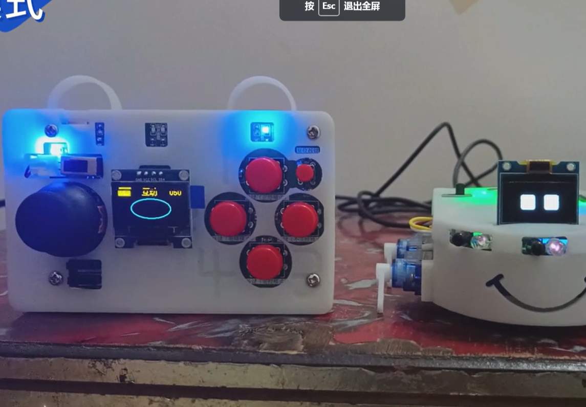
The robot is driven by four servo motors and uses an OLED display (using an SMT32F103C8T6 chip, running the RT-Thread operating system Nano version, based on Wildfire's book on RT-Thread and the project template created by Jiangxie Technology). Remote control uses a joystick and buttons for mode switching and motion control. It transmits and receives information via a 2.4G module (using an SMT32F103C8T6 chip, running the RT-Thread operating system Nano version, based on Wildfire's book on RT-Thread and the project template created by Jiangxie Technology).


VID_20240118_144558.mp4
Cute robot at low frame rate.mp4
The adorable quadruped robot KEIL project (standard library).zip
PDF_Adorable Quadruped Robot with 2.4G Remote Control.zip
Altium_Adorable Quadruped Robot with 2.4G Remote Control.zip
PADS_Adorable Quadruped Robot with 2.4G Remote Control.zip
BOM_Adorable Quadruped Robot with 2.4G Remote Control.xlsx
91378
Smart Greenhouse Monitoring System
The project uses the ESP32-C3 as its core to design an intelligent greenhouse monitoring system. Powered by solar panels and lithium batteries, it collects data on the greenhouse's temperature, humidity, VOCs, carbon dioxide, and light intensity, which is then uploaded to an Alibaba Cloud platform for display.
Project Description
: This project uses the ESP32-C3 as its core to design an intelligent greenhouse monitoring system. Powered by solar panels and lithium batteries, it collects environmental data such as temperature, humidity, VOCs, carbon dioxide, and light intensity within the greenhouse, uploading the data to an Alibaba Cloud platform for display. A 0.91-inch OLED display also shows the debugging data.
The PCB design uses LCSC EDA Professional Edition,
and the software design uses VS Code + ESP-IDF.
The following is the project framework diagram:

Project Functions :
1. Solar Power Supply System
2. Environmental Parameter Collection
3. Wi-Fi Network Interaction
4. Big Data Platform Display
5. OAT Remote Upgrade
Project Attributes:
This project is being publicly disclosed for the first time and is an original work by the author. This project has not won any awards in other competitions.
Project Progress:
PCB design completed;
Programming completed;
Casing design not yet started.
Design Principles:
I. Power Supply Section
1.0 Lithium Battery Charging Circuit :

Input is the positive and negative terminals of the solar panel (solar panel specifications 9V 2W). The lithium battery consists of two 18650 batteries connected in series. The system operating voltage is between 6V and 8.2V.
1.1 Lithium Battery Load Balancing

Control: The voltage of a single lithium battery cell cannot exceed 4.2V. This mainly serves as overcharge protection. When the voltage reaches 4.2V, the MOSFET turns on, consuming the voltage of a single lithium battery cell. When the voltage is less than 4.2V, the MOSFET turns off.
1.2 Lithium Battery Undervoltage Protection

: Monitors the battery voltage. If it is less than 6V, it controls the DC-DC step-down chip to enable, the system stops running, and waits for the battery to charge to above 6.47V before the system resumes power supply.
1.3 DC-DC Step-Down

II. Sensor Acquisition Circuit

III. MCU Main Control Section


IV. PCB Rendering


Software Description:
1. The MCU is ESP32-C3.
2. The coding software is VScode + ESP-IDF.

Blufi file: Bluetooth network configuration;
BSP file: Sensor data acquisition;
MQTT file: Server interaction data transmission;
OLED file: Motherboard 0.91-inch OLED display driver;
OTA file: OTA remote upgrade (in conjunction with Alibaba Cloud OSS management and control platform);
WS2812 file: Motherboard running indicator driver;

bsp_BH1750.c file: Ambient light acquisition;
DHT22.c file: Temperature and humidity acquisition
; KQM6600.c file: VOC gas acquisition (including carbon dioxide, formaldehyde, volatile organic compounds);
sensor file: Acquire environmental data.
SET button usage instructions:
Single click: Acquire and update data (viewable in the debug window)
; Double click: Update data to Alibaba Cloud platform;
Triple click: Send low battery alarm (meaningless);
Long press: Approximately 3 seconds. Start remote upgrade (the OLED screen will display the upgrade status).

For specific program details, please refer to the program source files . The physical image
shown

is the first initial version; the second version is currently being prototyped and has undergone minor adjustments (see the 3D image above for the second version). The schematic diagram above is the latest schematic diagram of the second version. There are many online tutorials for creating
IoT platform
devices; I found one, and you can search on Baidu for more information. Here are some screenshots of key pages:
Alibaba Cloud IoT Platform Setup - Bilibili (bilibili.com).


The corresponding program modification is in mqtt.c macro definition.

The image below shows the definition of the uploaded data type and function name.

After setting these, the motherboard connects to Alibaba Cloud and reports data every 2 minutes (low power consumption is not yet implemented). Data display can be seen in the IoT platform's object model data, showing the real-time upload status.

Big Data Platform Data Display
: Currently in its initial version, it implements data display, remote OTA upgrade, and other functions. The page has not been optimized
. Note: Because Alibaba Cloud IoT is used... The Studio module displays a big data platform, currently in public beta. It will be taken offline at the end of July; it's unclear if a test version will be available. Upgrading to the enterprise version costs 2K RMB per month, which is unnecessary for individual users. Note that without a test version, data can only be viewed on the aforementioned object model data page. This big data platform doesn't demonstrate


OTA remote upgrades .
Since remote upgrades use the IOT Studio component, and the public beta will be removed at the end of July, if no test version is available, remote upgrades will only work via the motherboard buttons; network-controlled upgrades will be disabled.


Design Considerations :
None
available. This section outlines some considerations for the project's creation (optional).
Other
Demo Videos: Upload demo videos as attachments. Attachments can be uploaded up to 50MB. Files larger than 50MB can be hosted on other cloud storage or video websites; simply include the link here. Project
Attachments: Entries participating in the event must upload project-related program attachments to an open-source platform or personal code storage cloud. Attachments can be uploaded up to 50MB (do not upload to the LCSC workspace, as there are limitations).
Sensor Procurement Link.docx
IOT_Board_V1.0 (program).zip
PDF_Smart Greenhouse Monitoring System.zip
Altium Smart Greenhouse Monitoring System.zip
PADS Smart Greenhouse Monitoring System.zip
BOM_Smart Greenhouse Monitoring System.xlsx
91379
2019_Question D_Simple Circuit Characteristic Tester
This simple circuit characteristic tester
analyzes data to obtain input and output resistance values, generates amplitude-frequency response curves, and performs fault detection. Relevant data, curve content, and fault analysis are transmitted via STM32 to a serial port display.
I. Problem Requirements


II. Design Analysis
This design mainly consists of a DDS module, a voltage RMS detection circuit module, a multi-channel AD conversion module (AD7606), a microcontroller, and a serial port display module. The FPGA controls the DDS module to generate the input signal, and the ADC module collects the signal under test after processing by the preceding circuitry and sends it to the FPGA for processing. The FPGA analyzes the obtained data and sends the relevant data to the STM32 microcontroller via serial port for further processing. Finally, the STM32 controls the serial port display to show the required data and waveforms.
III. Overall Design Block Diagram

IV. Hardware Circuit Composition
AD637 RMS Detection Module


Relay Module


Amplifier Circuit Module


V. Program Diagram
FPGA-RTL View:

VI. Physical Demonstration


VII. Attachments
Attachment 1: Program and Related Materials:
Baidu Cloud
Link: https://pan.baidu.com/s/1psOP4jlj3Zlo8JmQT7jVSw?pwd=2grw
Extraction Code: 2grw
-- Shared by Baidu Cloud Super Member V5
PDF_2019_Question D_Simple Circuit Characteristic Tester.zip
Altium_2019_Problem D_Simple Circuit Characteristic Tester.zip
PADS_2019_Question D_Simple Circuit Characteristic Tester.zip
BOM_2019_Question D_Simple Circuit Characteristic Tester.xlsx
91380
Old door locks were upgraded with Wi-Fi and fingerprint recognition modules.
This module was custom-developed to address the issue of the structure of old-style steel doors in homes being unable to use commercially available smart door locks.
Project Introduction for Adding WiFi and Fingerprint Functionality to Old-Style Door Locks:
This module was custom-developed to address the incompatibility of commercially available smart door locks with older steel door structures. The hardware utilizes an ESP32 C3 as the main controller, a BM2166 circular fingerprint module, and a 30kg servo motor as the actuator. The power supply features a dual-power automatic switching design, allowing uninterrupted switching between internal and external power. A 3000mA battery is included to handle unexpected power outages. To prevent brute-force fingerprint attacks, the system is designed to verify the unique device code of the fingerprint module each time it is unlocked. Fingerprint matching is at its highest level; multiple incorrect fingerprint matches will lock the module. The system has an automatic sleep function. When an external power outage is detected, the system automatically shuts off WiFi and enters ESP32 deep sleep mode. It is immediately awakened when a finger is pressed, performs a fingerprint recognition, and then enters deep sleep again. When external power is restored, WiFi is automatically activated to connect to the network, enabling remote unlocking.
The exterior of the door
uses a standard aluminum alloy handle. The fingerprint module is mounted on the handle via a printed component, with no exposed wires. The module is installed at a 30° angle, allowing for comfortable fingerprint scanning with the thumb, completing the entire process from fingerprint recognition to unlocking the door in one step.

Inside the door:
a servo motor is used for a flexible connection to the lock body structure via a cable, without hindering manual operation. The 30kg servo motor can handle virtually any pull on the lock. I used an acrylic sheet to fix it to the door, but the back of the structure is a flat surface and can also be secured with 3M double-sided tape.

Regarding power:
Since this design is based on my home's situation, with a power outlet near the door, it primarily uses an external power source, with a battery as backup. I usually use it plugged in.

However, thanks to the ESP32's excellent power management, the battery life is also quite good. In sleep mode: 4.7mA with the servo motor connected, and 81uA without. A 3000mA/h 18650 battery provides a long battery life.


Note: Only the hardware portion of this project is open source. The first generation of this project was completed in early 2021, using an STM32 as the main controller, and it has been working flawlessly ever since. The fingerprint module was the only circular fingerprint module available at the time, and it seems to be discontinued now. Other circular modules work on a similar principle, though the wiring order might need adjustment. Therefore, the model and program will not be open-sourced.
There are currently two versions:
1. The standard version, which is the one shown in the picture that I have successfully tested using a PCB.
2. An improved version with added voltage recognition and servo power-off circuits. The improved version is more suitable for battery-only solutions, as it can detect low battery levels and provide an alarm for timely battery replacement or charging. However, I haven't tested it; for me, the standard version is sufficient.
db0baeaddff71314fb3e179826caa074.mp4
PDF_Adding WiFi and Fingerprint Recognition Modules to Old Door Locks.zip
Altium - Add WiFi and fingerprint recognition module to old door locks.zip
PADS_Add WiFi and Fingerprint Recognition Module to Old Door Locks.zip
BOM_Adding WiFi and Fingerprint Recognition Modules to Old Door Locks.xlsx
91381
ESP32 Weather Clock and SD Card MP3 Playback
Weather clock on ESP32 and MP3 playback from SD card

Materials used: ESP32 + MAX98357 + 1.69-inch touchscreen CST816 driver Project environment: ESP-IDF + ESP-ADF + LVGL Project progress: The weather clock interface was completed using the development board (see image).
Project description:

1. Connect to WiFi. On first use, you can choose to scan for WiFi networks; the screen will display the found WiFi networks for manual connection.
2. After successful connection, the WiFi username and password will be saved to NVS. Subsequent connections do not require scanning.

3. A weather clock interface created using LVGL can display the time and weather for today and tomorrow, and also has a scrolling suggestion. City names can be manually entered.

4. A music playback interface was created using LVGL and ESP-ADF to play MP3 files from an SD card,

with functions such as next track, previous track, pause, playback progress bar, progress bar dragging, and selecting specific songs.
Full video demonstration available on Bilibili: BV1Se411m7B3
##############Note#########
If the ESP32 screen doesn't fit, do not force it in. Do not force it in. Try to sand it down. Don't break the screen! 555555555555555555555
Updated January 16, 2024:
Added the ability to play three favorite online radio stations to the MP3 interface. The "Warm Winter Creations" ZIP file was also re-uploaded.

video_20240104_155157.mp4
ESP32 Box_2.STL
esp32 cover.STL
Warm Winter Creations.zip
video_20240116_121732.mp4
PDF_esp32 Weather Clock with SD Card MP3 Playback.zip
Altium_esp32 Weather Clock with SD Card MP3 Playback.zip
PADS_esp32 Weather Clock with SD Card MP3 Playback.zip
BOM_esp32 Weather Clock and SD Card MP3 Playback.xlsx
91382
DS-ESP32_DISPLAY Color Screen Printing
The ESP32 power controller board controls the power on/off function of the product, and also has 3 WS2812 color light controller interfaces, 2 LED driver controls, etc. This solution is currently the power control board for a Bluetooth speaker that I made myself.
I. Product Introduction: The ESP32 power controller board controls the power on/off function of the product. It also features three WS2812 LED controller interfaces and two LED driver controls. This solution is currently used in a self-developed Bluetooth speaker power control board.
II. Board Functions: 1. Power control: Supports 24V power input and touch-button power on/off. 2. Three WS2812 LED strip driver interfaces, also includes a microphone for volume control, enabling a microphone-based lighting effect. 3. Two LED dimming drivers for desktop lamp control and illumination. 4. Features a photosensitive acquisition circuit. 5. One SPI LCD screen driver interface, which can be used as a desktop weather clock display. 6. The board is powered by a voltage below 24V and has two DC step-down circuits to power the LED strip and MCU.
III. Rendering of the DS-ESP32 controller board:
1. 3D image of the front of the PCB.

2. Color silkscreen image of the back of the PCB. 3.

Photo of the PCBA.

IV. Circuit description and usage introduction: 1. This project is a control board for a Bluetooth speaker. The physical product has been completed. The main controller of the control board uses Espressif's ESP32-D0WD-V3 chip, with an external 8M flash. A simple speaker pickup light effect has been implemented. This project can realize the power-on and power-off function through an external touch button switch. Whether to provide power to the Bluetooth amplifier board (which uses the previously open-source TPA3116 Bluetooth amplifier solution) is also discussed. The simple power-on and power-off function of the amplifier system is now implemented.
2. Power Amplifier Power-On/Off Control: The circuit diagram is shown below.

A 24V power input is used, controlled by a P-MOS transistor. When the ON/OFF button is pressed, PVCC+ conducts, powering the chip and turning on the MCU's P_ON for continuous power-on. Power-off is achieved by pressing and holding the ON/OFF button for 3 seconds. The MCU determines the P_SW press duration and turns off the MCU's P_ON.
Additionally, in the power-on state, a light touch of the button controls the WS2812's LED effects, switching between different LED strip effects.
3. Microphone Pickup for Sound and Light Synchronization: This solution is based on the microphone-light scheme from the previous HACK Labs project, but due to its complexity, it didn't achieve the desired effect. This project only needs to pick up sound after volume playback to drive the two rows of LED strips on my Bluetooth solution. A screenshot of the Bluetooth speaker's main view is shown below. An acrylic chassis rendering is also included. The effect diagram is as follows:


4. The board also has an LCD display interface for connecting an external SPI color screen. In this project, I designed a 1.54-inch LCD for a simple clock display. Because this involves a color screen driver, and due to my limited software skills, I have temporarily shelved this function. I also hope that interested software developers will collaborate with me on the development; I will provide hardware support free of charge.

5. The board also reserves two LED drivers for general desktop lighting. It will be convenient to add a desk lamp later. The reason for two channels is that one controls white light and the other controls warm white light. This makes it easier to add control functionality to my desktop when soldering products later.

V. Product Test Video
ed6f122a80e524f34c231b582df09eb4.mp4
c734eeb644af29767994450d43117cd7.mp4
PDF_DS-ESP32_DISPLAY Color Silkscreen.zip
Altium_DS-ESP32_DISPLAY Color Silkscreen.zip
PADS_DS-ESP32_DISPLAY Color Silk Screen Printing.zip
BOM_DS-ESP32_DISPLAY Color Silkscreen.xlsx
91383
Integrated brushless motor FOC control drive board 1.0 Nazarite-Turbo-Drive brushless ESC
Nazarite_Turbo_Drive, an integrated brushless motor control driver board,
is Rcer's last stand! A self-developed FOC driver board.

Project Musings:
In my freshman year, as a team member, I participated in the National Robotics Competition with senior students and won a national first prize (11th place nationwide). At that time, I was still a newbie following along with the senior students, doing wiring, layout, soldering, and playing with oscilloscopes and load meters. In my sophomore year, as a key member and the leader of the hardware group, I participated in RoboCon and won a national first prize (this time, 5th place nationwide!!!). At this point, I was promoted to a big newbie, haha. I especially remember going to Nanjing University of Science and Technology during the summer to participate in the RoboCon National Robotics Competition. I saw many universities able to develop their own Foc driver boards, and the finished products always looked enviable to me, haha. As a newbie, but a newbie also has dreams, and I also hope to make my own Foc driver board. The RoboCon National College Robotics Competition is a robotics competition with high rule complexity, strong competition, high difficulty in comprehensive robot design, and involves collaboration across multiple disciplines. In robotics competitions, where rapid turning, agile operation, high-precision control, and high-response control are required, how to fully leverage performance advantages and efficiency is crucial. Sensorless FOC-based brushless motor vector control is undoubtedly the best control method. However, to adapt to brushless motors with different parameters and meet the high bursts and high response speeds of competition scenarios, a more compatible brushless motor control driver is needed. Furthermore, both hardware circuit design and software FOC algorithm design present significant challenges. This paper proposes a self-developed hardware circuit system design that integrates the controller and driver. The pre-driver chip uses TI's high-current gate driver DRV8301, and the selection of advanced MOSFETs and precise current sampling with three resistors are employed. In terms of software design, the characteristic of sensorless control is that the motor rotor position and speed information comes from an estimator rather than sensors. This paper utilizes MATLAB/Simulink... Simulation software is used to construct a simulation model of a sensorless control system for a brushless DC motor based on the extended EKF (Extended Kalman Filter) algorithm, enabling parameter identification and acquisition. It is also compatible with the host computer debugging function of Benjamin VESC, a leading brushless ESC in the industry. It can utilize the sensorless FOC algorithm to leverage the advantages of brushless motor control, such as high precision, high efficiency, low noise and vibration, high response speed, and protection functions, making it highly valuable in robotics competitions.
At the Robocon National Undergraduate Robotics Competition, the adoption of differential steering wheel robot chassis designs by universities is gradually becoming a trend. The selection of motors for the drive wheels with different torques, KV values, and power, within the increasingly common rules governing the overall size of robots, has become a crucial consideration for universities. Consequently, the demand for encoder-based sensor-based brushless FOC control for the matching motors has emerged, shifting towards encoder-free sensorless FOC control. This approach not only satisfies the need for size advantages but also effectively integrates the mechanical and electrical control structure of the robot design, leveraging structural advantages, while providing high-response, high-precision control for the steering wheel chassis motors to better meet the speed-driven requirements of competitive events. However, technical exchanges among universities have revealed that most universities with weaker foundations and experience, after selecting motors with different power requirements, primarily use the two best-known foreign brushless ESCs in the industry: Benjamin VESC and Odrive. Due to their high performance, rich data display functions, and user-friendly interface and configuration tools, they have become the preferred drivers for most universities. However, these controllers are expensive and have low maintenance rates. Often, due to protected firmware code and erased hardware parameters, damage to the driver is irreparable, leading to stockpiling of large quantities in laboratories. Therefore, developing a high-performance brushless motor controller became a primary research task for the laboratory. Building on the accumulated advantages of three years of brushless ESC research and development in our laboratory, this paper proposes a sensorless FOC-based integrated brushless motor control driver system design. Self-developed versions of hardware and software designs are presented. Based on the different load parameters required for brushless motor control in our laboratory's robot structure, the basic circuit structure of the brushless ESC is deeply optimized in the hardware design, and the extreme parameters, substitutability, and cost control of key circuit components are selected to achieve high-power design. In the software design, motor parameter information is acquired in a sensorless manner. This paper utilizes an extended Kalman filter observer for model building, while also being compatible with the Benjamin VESC's host computer debugging function to fully meet motor debugging compatibility requirements. This integrated brushless motor control driver can achieve a peak power of 300W with an input voltage of 6S. It effectively solves the bottleneck problem of key core technologies and has wide applications in laboratory development and in scenarios requiring ultra-high drive power, high precision, and high response, such as robot joints and motion chassis.
Easy Introduction to FOC Algorithm:
1. FOC Vector Control Principle
1.1 Overview and Control Flow of Field-Oriented
Control FOC (Field-Oriented Control), also known as "vector control" in the industry, calculates the voltage vector required by the sector and uses SVPWM technology to generate a sine wave signal with a 120° phase difference between the three phases required by the three-phase brushless motor coils, driving the inverter circuit and thus driving the motor. FOC aims to achieve efficient and precise control of brushless motors. Brushless motor control progresses from sensored square wave -> sensorless square wave -> sensored FOC -> sensorless FOC. As one of the optimal control methods for efficient control of brushless DC motors (BLDC) and permanent magnet synchronous motors (PMSM), FOC vector control offers several significant advantages over square wave control. These advantages include smooth torque output, reduced resonance noise and vibration, precise control of motor angle and output torque as needed, higher efficiency, and lower power consumption. Furthermore, FOC control maintains stable performance under zero-speed, high-traction start-up of the steering wheel, and its closed-loop feedback allows for monitoring of the motor's actual state. To better understand the principles of FOC vector control, we first examine its control signal flow graph, then the coordinate transformation principle. Through Park transform, Clark transform, inverse Park transform, SVPWM algorithm, and the determination and judgment of space vector sectors, "pixel-level" control of the motor can be achieved.

Figure 1: Block diagram of brushless motor field-oriented control.
In the FOC algorithm, essentially, we
1.2 Park Transform and Inverse Park Transform.
The Park transform, also known as the dq coordinate transform in field-oriented control, is a
matrix . It can be used to transform the dimensions of three-phase motor parameters (such as phase voltage, phase current, and field-oriented information) in the stationary coordinate system to the rotating dq coordinate system. The purpose of the Park transform is mainly to achieve two key aspects of control: ① The projections iα, iβ of the three-phase AC currents ia, ib, ic on the two-dimensional coordinate axes α and β are equivalently transformed to the dq coordinate system. This decouples the motor's current signal into the direct axis (d-axis) and the quadrature axis (q-axis), providing two parameters iq, id for position estimation. The d-axis direction coincides with the rotor flux direction, and the q-axis direction is perpendicular to the rotor flux direction, thus enabling field depth control, aligning the motor's magnetic field with the d-axis, and maximizing the output torque. ② The output torque of the motor can be controlled by controlling the current along the q-axis. Essentially, the Park transform decouples the amplitude and angle of a highly coupled, difficult-to-control nonlinear system through coordinate matrix transformation, converting a conventional nonlinear system into a linear system for control, thereby achieving excellent dynamic control performance.

Figure 2: Conversion of a two-phase stationary coordinate system to a two-phase rotating coordinate system.
The essence of the Park transform is to transform the stationary αβ-axis coordinate system into a rotating dq-axis coordinate system through mathematical formulas. The dq-axis coordinate system always rotates with the rotor, meaning the goal is to control an AC motor using a linear system similar to that used for controlling a DC motor, thus obtaining two DC-dimensional components. θ represents the rotation angle of the rotating coordinate system relative to the stationary coordinate system. This rotation angle θ can be obtained in practical engineering operations through magnetic encoders or Hall sensors to acquire the real-time operating rotation angle of the motor. The rotation of the coordinate system in the corresponding mathematical formula involves the use of a rotation matrix. The matrix representation of the Park transform is obtained by multiplying the stationary coordinate system and the rotation matrix in a multiplier:

Figure 3: Park Transform Matrix Representation
. The inverse Park transform is the reverse operation of the Park transform, converting the voltage or current signal in the dq-axis rotating coordinate system into a signal in the αβ stationary coordinate system. This allows the output signals Vα and Vβ to be used as input signals for SVPWM to control the three-phase inverter circuit, thereby controlling the actual three-phase AC motor system. In other words, it converts the DC signals Vq and Vd of the front-end PI controller into sinusoidal signals, i.e., converting DC dimensional signals into AC dimensional signals. The corresponding matrix representation is shown in

Figure 4: Inverse Park Transform Matrix Representation.
Using Matlab's Simulink simulation function, the built-in application analyzes the signals, preprocesses the time domain, frequency domain, and linear system analysis to model and simulate the Park transform and inverse Park transform. The Park sub-encapsulation module establishes three inputs Iα, Iβ, and θ, and two outputs Id and Iq. The following figure shows the Simulink simulation model of the Park transform built in Matlab.

Figure 2: Block diagram of Park transform based on Simulink
. In the encapsulated submodule, matrix input functions are added to the Park transform module to solve for the mathematical formulas Id and Iq. For the parameters Iα and Iβ, the output of the Clark transform can be used as the input to the Park transform. When testing the Park transform module separately, a sinusoidal current can be injected by a signal generator as the input parameter. Simultaneously, an analog oscilloscope is connected to the back of the module to observe the waveform generated by the Park transform, as shown below.

Figure 2: Output waveform of Park transform based on Simulink .
Similarly, three input parameters are added to the inverse Park module: Vd and Vq in the dq coordinate system, the angle value θ, and the two generated output parameters Vα and Vβ. These three signals are combined to facilitate module linking and import into the function module tool. The matrix transformation mathematical formula of the inverse Park transform is used to solve for Vα and Vβ. The following figure shows the Simulink simulation model of the inverse Park transform built in Matlab.

Figure 3: Sub-block diagram of the inverse Park transform module based on Matlab/Simulink.
In the inverse Park transform, since Vd and Vq are linear constant input DC signal parameters in the rotating coordinate system, the proposed angle information is generated by a signal with a period of 0.1 and an output phase range of 0-2π. Given that the current value Vd = 0 and Vq = 1, the signal flow is transformed into Vd and Vq. After the inverse Park transform and under the tuning of the angle information, the two DC information signals are superimposed on the angle information, converting into two sinusoidal AC waveforms with an amplitude of 1 and a phase difference of 90° along the α and β axes. The converted waveforms are shown in Figure

2: Output waveform of the inverse Park transform based on Simulink. Figure
1.3 Clark transformation and inverse Clark transformation:
Clark coordinate transformation is an important transformation in the FOC control flowchart. We need to understand why Clark coordinate transformation is necessary and how it differs from Park transformation. First, because magnetic field vector control requires the motor rotor to rotate continuously within one revolution, and the stator coils are 120° out of phase, it is necessary to rely on three-phase coils to simulate a continuously rotating magnetic field to drive the rotor to rotate. To generate a continuously rotating magnetic field, Faraday's law of electromagnetic induction must be applied, that is, the three-phase coils need to have sinusoidal alternating current to generate a continuously rotating magnetic field. In other words, the coils must be supplied with three-phase sinusoidal voltage to generate three-phase sinusoidal current to control the three-phase motor. The Clark transform decomposes the three-phase current and projects it onto the stationary ab coordinate axis to obtain ia, ib, and ic. It then transforms the input three-dimensional three-phase signal to obtain iα and iβ signals in a two-dimensional rectangular coordinate system (αβ coordinate system), which are then used as inputs to the Park transform. It can be understood that the collected three-phase currents ia, ib, and ic are three-phase AC currents. After the Clark transform, they are essentially sinusoidal AC signals on the α and β axes. At this point, the angle and amplitude information are not decoupled. However, true decoupling occurs when the current and angle information are used as the dq axis after the Park transform. This decoupling is then supplied to the PID controller for feedback control, forming a true closed loop. In summary, the essence of the Clark transform is to transform the spatial vector representation from a three-phase stationary coordinate system to a three-phase stationary coordinate system. The coordinate system is converted to a two-phase stationary coordinate system, as shown in

Figure 2. For the three -phase
currents Ia, Ib, and Ic of the brushless motor, the prerequisite for using them as input parameters for the Clark transformation is obtaining the motor's current parameters. This design uses a sensorless drive with three-resistance sampling, meaning that instead of using encoders or Hall sensors for three-phase current sampling, an observer is used to predict the motor parameter model. The corresponding values of Ia, Ib, and Ic are projected onto the abc axes of the coordinate system with a 120° phase error. Based on the direction projection calculation formula and the constraint of Kirchhoff's Law (KVL) Ia + Ib + Ic = 0, the mathematical expression for the rotation matrix using equal-amplitude transformation is shown in the figure below. The purpose of the 2/3 transformation coefficients for the Clark coordinate transformation is to obtain equal-amplitude variation coefficients based on the equal-amplitude variation of FOC.

Figure 4: Clark Transform Matrix Representation. The
Clark transform rotation matrix transformation formula is used in a function submodule using MATLAB/Simulink simulation tools. Three input quantities are Ia, Ib, and Ic, and two output quantities are Iα and Iβ. The simulation model is shown below:

Figure 4: Clark Transform Block Diagram Based on Matlab-Simulink.
The Simulink simulation block diagram shows that the three-phase currents Ia, Ib, and Ic, with a phase difference of 120°, acquired from the actual engineering design, are converted into two-phase sinusoidal AC currents Iα and Iβ by the encapsulated Clark transform submodule. The phase rotating coordinate system is transformed into a stationary two-phase coordinate system. The corresponding simulation result waveform is shown below:

Figure 2: Output waveform of Clark transform based on Simulink. The
inverse Clake transform is the inverse transformation of the Clark transform. The forward transform converts the three-phase current from the time domain to the αβ axis rotating coordinate system. In actual engineering, the α axis in the αβ coordinate system is aligned with the zero-sequence component of the current parameter by default, and the β axis is aligned with the positive and negative sequence components of the current parameter. Essentially, the two-phase sinusoidal current after the three-phase AC current is transformed is input into the Park transform, and the current and angle information of the dq axis are decoupled and separated, which makes it easier to input the parameter information into the PID for feedback. The inverse Clark transform plays the role of restoring the αβ components in the rotating coordinate system to the actual dimensions of the brushless motor in the time domain. It is worth noting that the Park transform and Clarke transform transform current, while the inverse Park transform and inverse Clarke transform transform voltage. The mathematical formula for their rotation matrix transformation is as follows:

Figure 4: Matrix representation of the inverse Clark transform. The
inverse Park transform is encapsulated in the Fcn function module of Matlab/Sumilink. The matrix representation of the inverse Clark transform is input to the Fcn module as the transformation function expression. The Iα and Iβ after the Clark transform are used as input quantities to obtain the three-phase AC current signals Ia, Ib, and Ic. The corresponding block diagram is as follows:

Figure 4: Block diagram of the inverse Clark transform based on Matlab-Simulink.
1.4 SVPWM modulation principle driving
SVPWM (Space Vector Pulse Width Space vector pulse width modulation (SVM) is a precise voltage output control based on vector control theory. A space vector is defined as a virtual vector generated during the control of a brushless motor. Compared to PWM (Pulse Width Modulation), which converts the input signal into a square wave pulse signal, a space vector is characterized by its ability to determine both magnitude and direction in space. In brushless motor drive methods, there are generally two types: trapezoidal wave six-step commutation drive and sinusoidal wave drive. In the operating principle of a synchronous motor, a sinusoidal alternating current with a 120° phase difference is typically applied to the three-phase stator windings ABC. This generates a composite rotating magnetic field, which drives the permanent magnet rotor's own magnetic field. The motor essentially rotates with this composite rotating magnetic field. The composite vector within the sector region is precisely the waveform obtained by controlling the output of the three-phase full-bridge inverter. The three-phase inverter is essentially a drive circuit composed of six upper and lower bridge arm MOSFETs, capable of converting DC parameters into AC parameters, i.e., generating a circuit where the current flow direction can be changed. Different voltages (currents) in different directions are applied at different times to drive the brushless motor. The three-phase inverter circuit is shown below:

Figure 4: BLDC three-phase full-bridge inverter circuit.
Its principle is to drive the motor by the conduction relationship of two pairs of MOSFETs. In order to prevent the upper and lower switches from forming a short circuit, the upper and lower switches of the same bridge arm must be complementary. Then, the full bridge composed of three half-bridges is recorded according to the conduction status. The total number of combinations of upper and lower bridge arm conduction is 000, 001, 010, 011, 100, 101, 110, 111. These 8 switch combinations correspond to six non-zero vectors in space, namely U1 (001), U2 (010), U3 (011), U4 (100), U5 (101), U6 (110) and two non-zero vectors U0 (000) and U7 (111). The zero space vector represents that the six MOSFET combinations cannot form an upper and lower conduction.
Project Hardware Circuit Introduction:

This project serves as an early attempt at an integrated brushless motor drive and control design. Some details may not be perfect, so please be gentle with your criticism. Below is a brief introduction to the design principles: Firstly, in terms of the overall hardware circuit: The integrated brushless motor control driver consists of a controller and a driver. The system hardware design includes a main control center unit module, a filter capacitor module, an LED indicator module, a crystal oscillator RCC circuit, a SW download circuit module, a reset circuit module, a Vcp driver Type-C analog serial port module, a CAN communication interface module, a DC-DC step-down module, a starting current-energy storage capacitor bank module, a high-side current sampling and detection module, an encoder interface, a three-phase full-bridge inverter circuit module, a pre-drive core control processor module, a radial IPS interface, an axial duct interface, a three-phase output interface, and a power input interface. Secondly, regarding the schematic design, the schematic is a culmination of information compiled from the following relevant materials. For those unfamiliar with FOC (Fan-Driver) technology, only introductory notes are provided (currently being updated), without answering specific FOC questions. For the most popular FOC driver boards both domestically and internationally, Benjamin and Odrive are widely recognized. As a hardware enthusiast, collecting numerous brushless motor driver boards is my responsibility and obligation (lol). Below are all the relevant materials I've studied. If you're interested, feel free to ask me questions in the comments. This open-source release only covers the hardware design; the software design is currently being packaged and organized. For


the minimum system circuit module, the main control unit chip selected in this paper is the STM32F405RGT6, used to provide drive control signals. This main control chip is a high-performance 32-bit ARM Cortex-M4 core microcontroller from STMicroelectronics, with a maximum clock frequency of 168MHz. It also integrates a hardware floating-point unit (FPU), has 1MB of FLASH and 192KB of SRAM, and can meet the requirements for storing complex FOC algorithm programs. Its rich peripherals, such as SPI, I2C, USART, and CAN communication interfaces, along with its 12-bit 16-channel ADC and 12 general-purpose 16-bit system timers, can meet the needs of integrated brushless motor control drivers. In the Robocon National Robotics Competition, where both hardware cost and processing performance are crucial, this model meets the requirements of lower cost and superior control.
The main control center utilizes three complementary PWM signal outputs: INH_A, INH_B, and INH_C from PA8-PA10, and complementary signals INL_A, INL_B, and INL_C from PB13-PB15. Internally, the complementary PWM signals are all output by timers. It employs one I2C communication channel (I2C2_SCLA and I2C2_SDA from PB10-PB11) for bidirectional communication with the radial IPS display module, and one CAN communication channel (CAN1_RX and CAN1_TX from PB8-PB9) for bidirectional communication with external brushless motors. Three channels (PC6-PC8, HALL1, HALL2, HALL3) are used for connecting to the Hall effect encoder. One SPI interface (PC9-PC12) is used by the main control unit to select the amplification factor of the internal current sampling operational amplifier when communicating with the pre-driver chip DRV8301DCAR. Three voltage monitoring channels (PA-PA2, corresponding to Voltage_A, Voltage_B, Voltage_C) are used for system voltage monitoring. Three current sampling monitoring channels (PC0-PC2, corresponding to Current_A, Current_B, Current_C) are used for system current sampling, providing reference parameters for the underlying current loop. Pre-programmed USB-USART bidirectional communication firmware (USB_DP and USB_DM) is provided, allowing connection via a Type-C cable to a graphical debugging tool (VOFA+) as a host computer, or control via the Benjamin VESC open-source VESC_Tool host computer. Through analog oscilloscope functionality and parameter display, various waveforms and motor speed, current, and other information can be displayed in real time during debugging. The minimum system circuit of the main control unit includes a two-pin passive crystal oscillator, which improves the oscillation stability of the external RCC clock. The download circuit uses a 4-pin LINK download method, with BOOT0 pulled low by default. Two LED test indicators are used to test whether the main control unit can be programmed normally.
Debugging the FOC algorithm for the brushless motor mainly focuses on whether the main frequency, timer, and current sampling module meet the requirements. The pre-driver chip DRV8301DCAR for the drive circuit requires three complementary PWM wave signals from the main control unit. The 12-bit ADC required by the current sampling high-side monitoring module has an accuracy of 1/4096, which meets the system monitoring requirements. The three-phase current generated by vector control will be acquired by the corresponding sampling module. The main control unit provides multiple programmable I/O ports for debugging. In summary, the STM32F405RGT6 chip fully meets the design requirements and can be used as the main control unit for an integrated brushless motor control driver. The following figure shows the control circuit of the main control unit.

The entire system's power management (PMU) is powered by a single 5500mAh TB47 DC power supply with a 6S lithium battery. The pre-driver chip DRV8301DCAR has a PVDD input voltage range of 6V-60V, powered by a DC power supply. The DRV8301 datasheet clearly states that it has an internal constant current source DC-DC chip with a built-in BST_BK pin. Only an external capacitor, inductor, and Schottky diode are needed to form a 5V step-down circuit. The 24V DC input voltage is automatically stepped down to 5V by the chip, and this 5V power supply will provide power to the encoder's external input interface. Therefore, this system's power module can reduce the need for a separate 24V-to-5V step-down power supply circuit. The main control unit, STM32F405RGT6, requires a 3.3V power supply; therefore, only one external step-down circuit is needed to power the main control unit. The main DC-DC step-down circuit is shown in the diagram below. The 24V input voltage can be provided with a 3.3V 3A output load capacity through the SY8089A1AAC. For the low-dropout step-down selection, this system uses a low-ripple DC-DC circuit instead of the commonly used LDO circuit. The selected DC-DC chip is the SY8089 from the RM-C development board, a driver chip from Silergy. The SY8089 and SY8089A are high-efficiency, high-frequency synchronous step-down DC-DC regulator ICs capable of providing up to 2A of output current. The SY8089 and SY8089A operate over a wide input voltage range from 2.7V to 5.5V and integrate the main switch and synchronous switch with extremely low RDS(ON) to minimize conduction losses. Low output voltage ripple and small external inductor and capacitor size enable switching frequencies greater than 1MHz. The SY8089 integrates short-circuit and overvoltage latch-up protection. Features include low RDS(ON) of the internal switches (top/bottom): 110mΩ/80mΩ. 2.7-5.5V input voltage range, 2A continuous, 3A peak load current capability, 1MHz switching frequency minimizes external components, internal soft-start limits inrush current, reliable short-circuit protection: SY8089: latch-up shutdown protection, SY8089A: hooded cup mode protection, reliable overvoltage protection: SY8089: latch-up shutdown protection, SY8089A: non-latching shutdown protection. Actually, this is all just background information. For hardware enthusiasts, mastering the selection of relevant inductors, fast recovery diodes, and feedback loops is sufficient.

The startup current-energy storage capacitor bank is used for buffering the power-on of the 6S high-voltage circuit, especially for the pre-driver chips required by the FOC driver board, such as FD6288, EG2134, IR2101, etc. For VIN power-on PVDD, low ESR and high ripple current are required. Here, we chose a yellow sapphire capacitor as the filter capacitor, paired with a 10uF small capacitor bank, forming a large capacitor + small power supply combination. Many interviewers like to ask, "Why not just use a single 22uF capacitor instead of two 10uF and two 100nF capacitors in parallel on the power supply? This would save PCB space." This is a relatively niche question, and the chances of it appearing in an interview are slim, but it's frequently used in practice. Generally, engineers with a few years of experience either understand this very well or overlook such small details. This discussion focuses on the insertion loss of the filter. In the 2MHz~300MHz target frequency band, the combination of 2x10uF + 2x0.1uF capacitors has a higher insertion loss than a single 22uF capacitor, making it more beneficial for power supply filtering. However, filter insertion loss is only one dimension of this analysis; other interpretations exist, such as the capacitor's frequency impedance curve. Simulation comparison and verification: Some might mention the capacitor's frequency impedance curve, but we won't discuss that today. We'll analyze this from the perspective of the filter's S-parameters. We'll use Murata's online simulation software SimSurfing for verification. We assume the 12V power supply is generated by a Buck circuit with a switching frequency of 2.2MHz. To more clearly observe the comparison effect, we focus on the frequency range of 2MHz-300MHz for this power supply. Step 1: Build a simple filter circuit: 0.1uF + 10uF.

Observe the S21 (insertion loss) curve of this filter circuit, as shown in the figure below.

It might not be immediately apparent. What would happen if we combined the two 10uF and two 0.1uF units from the power supply into a single 22uF unit?
Step 2: Build another filter circuit with only 22uF:

Observe the S21 curve of the filter circuit again.

It is clear that the S21 curve of 10uF + 0.1uF has a greater insertion loss in the 2MHz~300MHz range. According to the impedance mismatch principle of filters, the higher the insertion loss of the filter circuit in the target frequency band, the better.
That is, 10uF + 0.1uF has a better filtering effect within a limited frequency band.
Step 3: Build another filter circuit: 2x0.1uF + 2x10uF.
Let's look at the S21 curve of the filter circuit. As shown in the figure below: Among the three schemes, in the 2M~300MHz range, 2x10uF + 2x0.1uF has the highest insertion loss,


 京公网安备 11010802033920号

 102-624-02S-P31-B12


