Bilibili video introduction: --> Click to view.

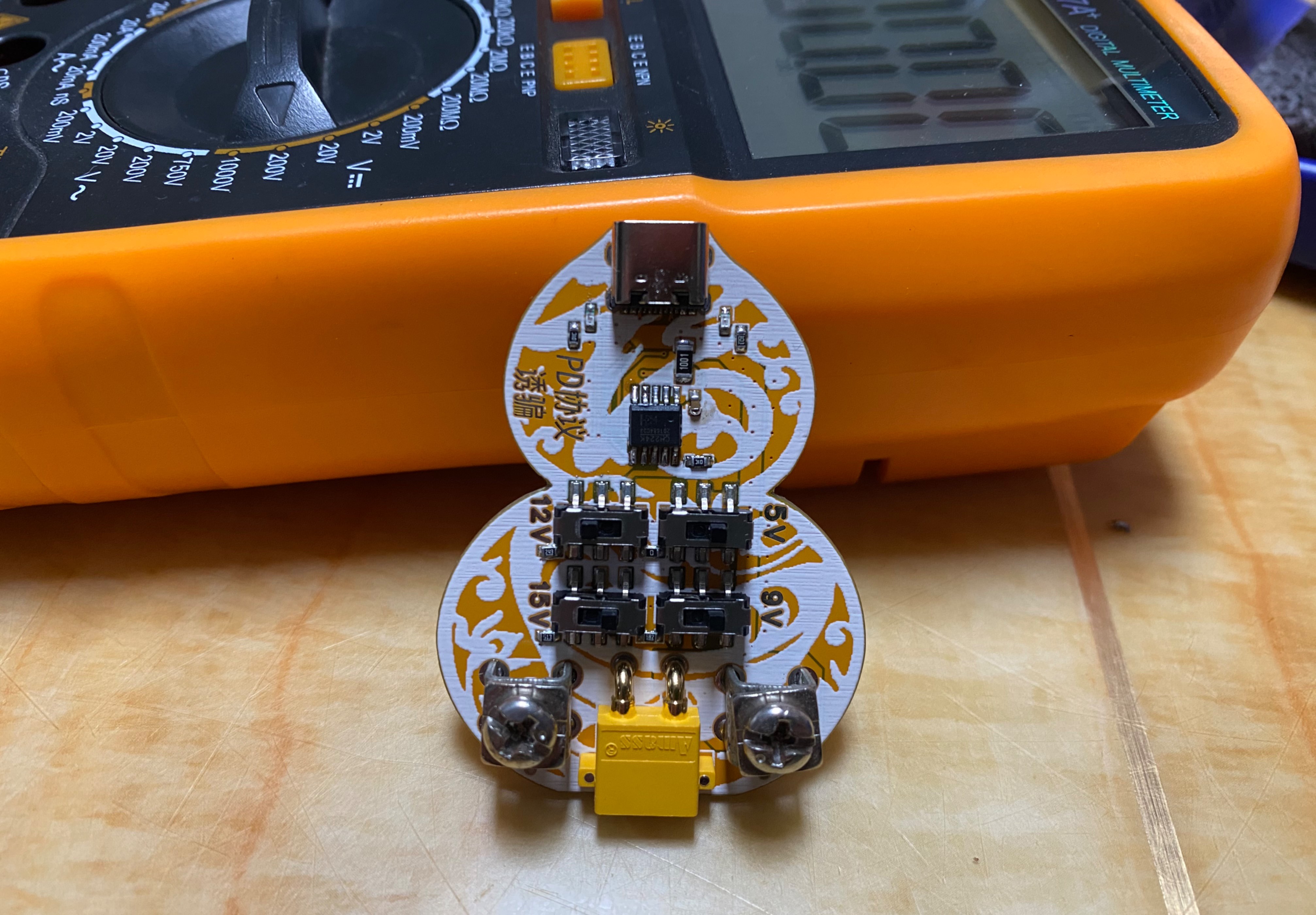
Using a CH224K charger with a PD-compatible charger
to induce 5V, 9V, 12V, 15V, and 20V voltages.

R9 is a current-limiting resistor. Since at 20V, I=V/R=(20-3.3)/1000=16.7mA, approximately 279mW of power, a 1206 package was used.
LED1 is a power indicator light, used to determine if the charger is outputting voltage.
LED2 will light up when the voltage reaches the set value, indicating whether the expected voltage has been reached.

PDF_PD Protocol Charger Output Voltage Deception ch224k.zip
Altium_PD protocol charger output voltage deception ch224k.zip
PADS_PD protocol charger output voltage deception ch224k.zip
BOM_PD Protocol Charger Output Voltage Deception ch224k.xlsx
91413
STM32-based colorful snowflake light design with LCD display
Modified from the open-source repository https://oshwhub.com/001_han-dan-xue-yuan/diy-guang-dian-she-ji-dong-yu-kuai-xue-hua-deng
Here are the pictures!
![IMG_2522.JPG]

![IMG_2523.JPG]

Red version: ![WeChat image_20231006113533.jpg]

White version ①:
![2.jpg]

![3.jpg]

![5.jpg]
White version front (with control chip STM32F103):
![IMG_2503.JPG]

![IMG_2506.JPG]

White version back (with control chip STM32F103):
![IMG_2504.JPG]

White version lit up:
![1.jpg]

![2.jpg]

![3.jpg]

![4.jpg]

Demo video (without control chip) link ①
[https://www.bilibili.com/video/BV1Wh4y1h7GB/?spm_id_from=333.999.0.0](https://www.bilibili.com/video/BV1Wh4y1h7GB/?spm_id_from=333.999.0.0)
Demo video without control chip link ②
https://www.bilibili.com/video/BV1A84y1S73s/?spm_id_from=333.999.0.0&vd_source=546381e542a881103bc2fe462ebe6317
Demo video without control chip link ③
https://www.bilibili.com/video/BV1X84y117fu/
Demo video with control chip link ⑤
https://www.bilibili.com/video/BV1Qp4y1M7ZV/
Hardware design description:
1. Several PCBs have been designed and tested under this project and are usable. Since the board has a large number of 0603 packaged LEDs, SMT is recommended. Choose the appropriate LED color according to your color requirements.
2. Constant current source power supply is recommended; otherwise, the integrated 5V to 3.3V LDO on the board may overheat.
4. You can choose not to use the LDO converter chip and directly power via Type-C.
5. There is a DXF file in the project. When importing, you can set its size to get snowflake lights of different sizes.
6. The light without a control chip has good brightness and looks quite nice, suitable as a room decoration. For
the model with a control chip:
1. Due to the current-limiting resistor, the microcontroller's output capability is low, and the presence of multiple LEDs results in very weak LED illumination. If using this circuit design, please remove the current-limiting resistor.
2. The circle in the middle of the screen was originally intended for a 1.69-inch circular LCD, but the hole was too small, preventing the inclusion of some functions.
3. SMT soldering is recommended for LEDs. It's best to use the same type of LED; otherwise, some LEDs may not light up.
Software design notes:
For models with integrated chips, programming is required. For models without integrated chips, a constant current source can be used for power supply.
The program for models with integrated chips is attached; the main functions are in the led.c file
! ![Snipaste_2023-10-10_17-47-38.jpg]

If using this design, it is recommended to use other control chips to reduce design costs.
The snowflake LED outline file has been uploaded. Import the DXF file when drawing the PCB to generate the corresponding PCB outline
.
Snowflake light frame file.dxf
Snowflake Light Control Test Program.zip
PDF_Design of a Colorful Snowflake Light with LCD Display Based on STM32.zip
Altium-based STM32 microcontroller with LCD display: Colorful Snowflake Light Design.zip
PADS_STM32-based Colorful Snowflake Light Design with LCD Display.zip
BOM: Design of a Colorful Snowflake Light with LCD Display Based on STM32.xlsx
91414
Intelligent storage box for electronic components
There are many types of electronic components nowadays, especially surface mount components, which require hardware engineers to spend a lot of time searching for. This project can realize intelligent storage of components, quick search and location, and component material status, with alarm prompts when there are insufficient components.
Project Description:
In the field of modern electronic engineering, there are numerous types of electronic components, especially surface-mount components. Engineers, particularly DIY hardware enthusiasts, often spend a significant amount of time searching for and locating these components. For example, I once was soldering a very simple PCB board with only five components, but I wasted an hour because I couldn't find the corresponding component. This component was rare and infrequently used, so I had it stored in a dark corner. Therefore, to improve engineering efficiency and reduce wasted time, I designed and developed an intelligent storage solution called the "Intelligent Electronic Component Storage Box." Intelligent

Electronic Component Storage Box Project Functional Topology Diagram
Features:
1. Intelligent Storage and Classification: This storage box, through its built-in intelligent system, can automatically identify, store, and classify various electronic components, especially surface-mount components. Each component is assigned a unique storage location, ensuring the entire inventory is organized.
2. Quick Search and Location: Users can input relevant component information, such as model and specifications, through a convenient interface. The system will quickly locate and display the component's storage location. This greatly reduces the time spent searching in the component library.
3. Real-time Component Status Monitoring: The storage box is equipped with sensors and a monitoring system that can monitor the quantity and status of components in real time. Users can check inventory status at any time to ensure sufficient components. When a component is insufficient, the system will automatically issue an alarm to remind the user to replenish it.
4. Unlimited Expansion with Left and Right Smart Boxes: The smart storage box has RS485 interfaces on both sides, allowing for wired cascading and wireless Bluetooth networking expansion.
5. Adjustable Height: Each layer of the smart storage box uses spring-loaded pins for power and data signal transmission, allowing users to decide the desired height based on their needs. (Currently, my maximum design height is five layers, which fits exactly five PCBs in one batch.)
6. Data Recording and Analysis: The storage box records each component storage and retrieval, and users can query historical records at any time. This not only helps in analyzing component usage but also helps users optimize inventory management strategies.
7. Convenient Mobile App Operation: The storage box features an intuitive and simple user interface, making operation more convenient. Users can manage components via a touchscreen or connected mobile devices.
Application Areas:
1. Electronic Hardware Development Companies: Improves the work efficiency of hardware engineers, reduces component search time, and accelerates product development cycles.
2. Electronic Manufacturing Plants: Manages and optimizes raw material inventory, reducing the risk of production line shutdowns due to component shortages.
3. School Laboratories: Provides laboratory personnel with a convenient and efficient component management method, reducing experimental time costs.
4. DIY Enthusiasts: Those who lack the time to manage and manage these tiny, delicate components.
Open Source License:
CC BY-SA 3.0
Project Functions
: 1. Component Storage:
Components are stored in designated locations using a mobile phone controlled by indicator lights in the component storage compartment, and their location information is recorded.
2. Quick Search and Location:
Users input component information, such as model and specifications, through the mobile application.
The underlying STM32 microcontroller responds to the query request, quickly locating and reporting the component's storage position through the mobile application's control system.
3. Data Recording and Analysis:
The mobile application can store a database, recording each component access.
Users can query historical records through the mobile application to analyze component usage.
4. Mobile application interface design:
Provide a user-friendly mobile application interface, including functions such as component query, storage and retrieval, and inventory monitoring.
Achieve stable and reliable communication with the STM32 development board via Bluetooth or Wi-Fi.
5. Auxiliary functions:
The top of the smart storage box has 25 RGB lights, which can be used as a night light, and the color and brightness can be freely switched by rotating the encoder.
Music rhythm mode: There are two RGB lights on the side of each layer of the smart storage box, which can follow the changes of external sound to form a rhythmic jump.
Project attributes:
Original work by the author.
Project progress :
The underlying hardware and mobile APP software are basically completed, and the APP software functions still need to be slightly improved and optimized.
Design principle:
The entire project mainly includes the design of the underlying hardware circuit and the design of the upper-level APP software. The underlying hardware uses four boards, each board is responsible for its own control task, and the upper-level APP software communicates with the underlying main control board via Bluetooth to realize the protocol data interaction between the underlying and upper layers.
1. Underlying hardware design principle
(1) Main control board:

The main function of the main control board is to provide the component position prompt. The schematic uses the WH-BLE106 low-power Bluetooth chip from Youren Technology, supporting Bluetooth wireless networking (up to 8 connections). The Bluetooth chip connects to the STM32F103C8T6's serial port 1. After receiving the protocol from the upper-layer APP, the microcontroller parses the component location information and outputs a PWM signal to control the RGB LEDs to turn on or off, providing component location indication. Each time, three RGB LEDs are used: two to indicate which floor a component is on, and one to indicate which row and column it's in. The underlying algorithm determines the correspondence.
Other functions include displaying Bluetooth connection status, component location, music rhythm, and a night light function on the OLED screen.
RS485 wired communication and power cascading are reserved on both sides, using 4-pin spring connectors for magnetic expansion connections.

3D rendering of the main control board
(2)

The core board of the display panel controls the data to be displayed on the OLED screen through the IIC protocol. There is also a rotary encoder, which is mainly used as a function button to facilitate switching the functions of the electronic component smart storage box, as well as changing the color and adjusting the brightness of the night light. All of these can be solved by a rotary encoder, which is very convenient to operate.

3D rendering of the display panel
(3)

The schematic diagram of the upper RGB board mainly connects 25 WS2812B lights in series. This is why I chose this RGB light. Only three wires are needed (power line 5V, ground line, signal line) to wirelessly expand the RGB light, and only one wire is needed. The signal line of the upper RGB board here is connected to the PB0 pin of the core board, which supports PWM+DMA fast output (TIM3 CH3).

3D rendering of the upper RGB board
(4) The

design principle of the back RGB board is similar to that of the upper RGB board. However, in order to facilitate the expansion of the height of the electronic component smart storage box, the signal line and power line use spring pins to freely connect the upper and lower floors. The signal lines on the rear RGB board connect to pin PA6 of the core board, supporting fast output (TIM3 CH1).

Rear RGB board 3D rendering
2. Upper-layer APP software design principles.
The Android software primarily utilizes Bluetooth Low Energy communication, enabling data interaction between the lower and upper layers through a predefined data protocol.
The upper-layer software mainly features the following interfaces:
1. Main Interface:
Displays the overall storage status of the current storage boxes.

2. Add Components: Allows
adding components and recording their physical location. Location messages are sent to the lower layer, triggering indicator lights.

3. Component Details:
Displays detailed information about components, allows for component retrieval, and sends location messages to the lower layer, triggering indicator lights.

4. All Components View
: Displays all electronic component smart storage boxes, including previously used ones.

5. Component Location Distribution:
Shows the distribution of all components on a floor at once. Clicking on a component leads to its details page.

6. Component Search:
Allows for fuzzy matching searches to quickly find and retrieve the desired components.

7. More Interfaces

8. PCB Project Management
Classifies and manages the electronic components required for each hardware project, enabling quick retrieval of needed components and improving efficiency.

Project Management Functions

Project Component Information Viewing
3. Appearance Design
Drawn using SolidWorks software, the overall appearance is as follows.

Assembly Front

Assembly Back
Software Description
The mobile APP and the underlying device communicate wirelessly via Bluetooth. Almost all the logic operations and data storage for the entire project are handled on the mobile APP, because Android allows for easy CRUD operations on the database. Complex storage within the underlying chip would be too difficult. Component information on the Android side is stored in a local database. When we perform component searches or storage operations on the mobile APP, the mobile APP will ultimately call Bluetooth communication to send the component's location information to the underlying MCU via a protocol. The underlying MCU's serial port is connected to the Bluetooth device. When the Bluetooth device receives the message from the mobile APP, the MCU will parse the protocol according to the message to deduce the component's location. Finally, the MCU controls the RGB light at that location to flash as a reminder. This is roughly the communication logic between the underlying and mobile software, and it's relatively simple and easy to understand.
Physical Demonstration:
1. Side view of the smart storage box for electronic components

; 2. Back view of the smart storage box for electronic components

; 3. Top view of the smart storage box for electronic components;

4. Open view of the smart storage box for electronic components

. Design Notes:
Due to time constraints, the shell was 3D printed, which was a slow process. Therefore, only a single smart storage box for electronic components is shown, which is only two layers high. If you want to replicate it, it can be up to five layers high, as the app software is designed for a five-layer height. Therefore, one smart storage box can store a maximum of 25 * 5 = 125 components. It can be wirelessly cascaded, up to a maximum of 8 units.
Other
Bilibili videos:
Smart Storage Box for Electronic Components Function Demonstration Video
3D Printed Shell.zip
WH-BLE106_V1.0.0.pdf
box.apk
box.hex
source code link.txt
Src code.zip
PDF_Electronic Components Smart Storage Box.zip
Altium_Electronic Components Smart Storage Box.zip
PADS_Electronic Components Smart Storage Box.zip
BOM_Electronic Components Intelligent Storage Box.xlsx
91415
FC3379 G2 USB flash drive
The FC3379, based on the QFN32 microcontroller, is a USB 3.0 controller that supports up to 1CE. It features dual BGA152 and TSOP48 pads, a double-layer board, and a G2 form factor.
First, some technical details:
This board doesn't have jumpers R5, R6, R7, and R8 for TSOP NVDDR2 because the new firmware supports automatic state switching. The VCCQ of the NAND flash memory is controlled by the controller software, eliminating the need for hard jumper switching; the controller will automatically adapt. However, the VCC power supply of the NAND flash memory cannot be switched by software, so jumpers R3 and R4 are designed to switch the VCC power supply of the NAND flash memory. R3=3.3V, R4=2.5V. The board has both BGA152 and TSOP48 pads. For the BGA152, I only connected the CH0 cable, so it doesn't support 180° upside-down NAND flash mounting. This is so that even 2CE NAND flash memory with one failed CE can still use this board, preventing the failed CE from interfering with the normal CE, maximizing utilization. The TSOP is a standard TSOP, supporting NVDDR2. For smaller components, except for the VCC jumper which needs to be soldered with a 0-ohm wire, it's completely compatible with the green board, so you can move the board directly.
Why design this board?
A while ago, I bought some FC3379 controller boards (as shown in the picture) on a second-hand marketplace

. Unfortunately, they weren't the standard BGA152 design, so I could only use TSOP48 chips. Therefore, I decided to design my own controller board that supports BGA152. ↓↓↓ So I designed a BGA152-compatible version, using dual BGA152 + TSOP48 pads, matching all the components, and leaving plenty of blank space on the back for printing my favorite designs.


↓↓↓ Card opening test (the card opening tool can be found on the official website: http://www.szfirstchip.com/col.jsp?id=142)

↓↓↓ AS SSD speed test results ↓↓↓


Approximately 65MB/s write speed and 120MB/s read speed. This is a single CE HYV6. Next up is a picture of a small manufacturer's self-proclaimed Yangtze Memory TAS process NAND flash memory, also 1CE 64GB. That's all for now. Feel free to ask any questions in the comments! ヾ(≧▽≦*)
o

FCMptools_U3_20230811_2.1.1.0.rar
PDF_FC3379 G2 version USB flash drive.zip
Altium_FC3379 G2 USB flash drive.zip
PADS_FC3379 G2 USB flash drive.zip
BOM_FC3379 G2 USB flash drive.xlsx
91416
Battery Internal Resistance Tester Based on PY32F002A Microcontroller
Battery Internal Resistance Meter Made with PY32F002A Microcontroller
I bought some PY32F002AF15P6TU batteries from LCSC and built a simple battery internal resistance tester to test their performance. The measurement range has two settings: milliohms and ohms. The milliohm setting displays a range of 00.00 to 60.00 milliohms with a minimum resolution of 0.01 milliohms. The ohm setting displays a range of 0.000 to 2.000 ohms with a minimum resolution of 1 milliohm. The measured current is 20 mA. The voltage rating is mainly for single-cell lithium batteries. A low-voltage DC blocking capacitor was chosen; for batteries with higher voltages, the DC blocking capacitor at the amplifier output needs to be changed.
It can mainly be used to measure battery internal resistance, capacitance ESR, and current sampling resistor. The right side
of the hardware section

contains the common power supply and display components, which I won't go into detail about. I'll mainly introduce the signal section on the left. The microcontroller outputs a 1kHz PWM signal, which is converted to a sine wave after RC filtering. This sine wave then passes through a C15 DC blocking capacitor, is boosted to VCC/2, and then enters the U2.1 voltage follower.

After obtaining a sine wave boosted to VCC/2, it enters the constant current circuit U2.2. The sampling resistors are three parallel 100-ohm resistors, with a TVS protection op-amp. Then, a 1kHz AC signal is injected into the battery through four parallel 10uF capacitors.

Ports H3, H4, H5, and H6 are connected to a Kelvin four-wire test clip. H3 and H5 are current excitation ports, and H4 and H6 are voltage signal ports. The DC voltage of the battery is isolated by capacitors C43 and C44 (100NF capacitors), and only the 1kHz AC voltage is extracted. The voltage is boosted to 1.65V after the capacitors. The four transistors are used as diodes here, with lower leakage current than diodes.

Next, it enters an instrumentation amplifier composed of three op-amps, with a gain of 21x.

Then, it enters the U5 analog switch. The sampling is attenuated and then amplified to achieve the switching between two ranges. The advantage is that the two ranges have the same phase shift, so only one range needs to be calibrated. After amplification, it directly enters the microcontroller ADC.

The microcontroller section is relatively simple. PB3 outputs a 1kHz sine wave. PA0 and PA1 are shorted ADC ports, and PB0, PA7, and PA4 are SPI ports. H8 SWDIO and H9 SWCLK are SWD debug ports used for debugging and program downloading. PA2 and PA3 are button input ports.
The SWD debug ports are
H8 SWDIO and H9 SWCLK, and another

port is a four-wire GND test clip. The amplifier outputs + and + signals are connected to one clip, and negative and negative signals to another.


The software
is written in GNU ARM assembly language using the ARM-NONE-EABI compiler.
A timer outputs a 1kHz sine wave. PA0 and PA1 enable two channels of ADC sampling. Another timer is set to a 100kHz trigger frequency to trigger ADC sampling. After sampling, the data is transferred to memory via DMA. The DMA uses a cyclic mode to sample 1000 points. The SYSTICK timer is set to interrupt once every 10 milliseconds. The code below implements the above functionality.
__adc_dma: ldr r0, = 0x40020000 ldr r1, = 0x40012440 @peripheral address str r1, [r0, # 0x10] ldr r1, = 0x20000160 @memory address str r1, [r0, # 0x14] ldr r1, = 1000 @transfer quantity str r1, [r0, # 0x0c] ldr r1, = 0x35a1 @ 0x583 @ 5a1 @transfer mode str r1, [r0, # 0x08]
_adcchushihua: ldr r0, = 0x40012400 @ADC base address ldr r1, = 0x80000000 str r1, [r0, # 0x08] @ADC Control Register (ADC_CR) @ADC Calibration_dengadcjiaozhun: ldr r1, [r0, # 0x08] movs r1, r1 bmi _dengadcjiaozhun @ ADC Calibration_tongdaoxuanze: ldr r1, = 0x20000000 str r1, [r0, # 0x10] @ Clock Divider movs r1, # 0x03 str r1, [r0, # 0x28] @ Channel Selection Register (ADC_CHSELR) ldr r1, = 0x8c3 @0x3003 @Continuous 0x2003 @Trigger 0x8c3 @ 0xc43 @TIM3 0x8c3 @0x2003 @0x8c3 str r1, [r0, # 0x0c] @ Configuration Register 1 (ADC_CFGR1) movs r1, # 0 str r1, [r0, # 0x14] @ ADC Sampling Time Register (ADC_SMPR) ldr r1, = 0x05 @ Start Conversion str r1, [r0, # 0x08] @ Control Register (ADC_CR) str r1, [r0, # 0x08]
@tim3chushihua: ldr r3, = 0x40000400 @ tim3_cr1 ldr r2, = 0 str r2, [r3, # 0x28] @ psc ldr r2, = 959 str r2, [r3, # 0x2c] @ ARR movs r2, # 0x20 str r2, [r3, # 0x04] @ TRGO
@tim1chushiha: ldr r0, = 0x40012c00 @ tim1_cr1 movs r1, # 0 str r1, [r0, # 0x28] @ psc ldr r1, = 47999 str r1, [r0, # 0x2c] @ ARR @ movs r1, # 0x20 @ str r1, [r0, # 0x04] @ TRGO ldr r1, = 0x6800 str r1, [r0, # 0x18] @ ccmr1 CC2 ldr r1, = 0x10 @ CC2 str r1, [r0, # 0x20] @ ccer ldr r1, = 0x8000 str r1, [r0, # 0x44] @ BDTR @ ldr r1, = 0x100@CC2DMA@ str r1, [r0, # 0x0c] @ DIER ldr r1, = 24000 str r1, [r0, # 0x38] ldr r1, = 0x81 str r1, [r0] str r1, [r3] ldr r4, = 0xe000e010 ldr r3, = 479999 str r3, [r4, # 4] str r3, [r4, # 8] movs r3, # 0x07 str r3, [r4] @systick open
ldr r0, = lvbo_changdu ldr r1, = lvbo_youyi movs r2, # 200 str r2, [r0] movs r2, # 14 str r2, [r1]
ldr r0, = cossin ldr r1, =
After entering the SYSTICK timer interrupt, the real and imaginary parts of 1000 data points are calculated using DFT, and then each is entered into a 200-point sliding filter
. shangbi_r str r0, [r1]
ldr r0, = shangbi_r ldr r1, = shangbi_i ldr r0, [r0] ldr r1, [r1] bl __ji_suan_fu_du ldr r2, = fudu str r0, [r2]
ldr r0, = liangcheng ldr r2, = 0x50000400 ldr r3, [r0] cmp r3, # 1 beq __haoou_dang__ou_dang: movs r3, # 1 lsls r3, r3, # 16 str r3, [r2, # 0x18] b __systick_fanhui__haoou_dang: movs r3, # 1 str r3, [r2, # 0x18] __systick_fanhui: ldr r0, = 0xe0000d04 ldr r1, = 0x02000000 str r1, [r0] @ Clear SYSTICK interrupt pop {r0-r4,pc}
The DFT program uses a minimal loop approach, hence its length. I'm unsure if this is faster, but the space is plentiful.
Here we obtain the real and imaginary parts of the tested battery. First, clamp a non-inductive resistor, calculate the phase using ATAN2, then rotate the angle to 0 degrees to only show the real part, thus avoiding the influence of the test line inductance.
The phase rotation method, and the methods for ATAN2 and calculating COS and SIN, are detailed in the attached cordic.pdf.

The program between the function name anjian3 and ting is the calibration program, which mainly has three calibration items: short-circuit zeroing, phase calibration, and standard resistance calibration. It's quite long, so I won't post it here. The
calibration methods have three calibration menus: P-00 for short-circuit zeroing, P-01 for phase calibration, and P-02 for standard resistance calibration. Press and hold the switch button, then simultaneously press the other button to enter calibration mode. The digital display shows P-00. Pressing the up button will switch between P-00, P-01, and P-02. Pressing both buttons together exits the calibration menu, displaying END. Pressing the other button enters the displayed menu. P-00: The clip is short-circuited. Adjust both up and down buttons to 0. First, adjust the ohm setting, then press both buttons together to enter the milliohm setting. After adjusting, press both buttons together again to save to FLASH, displaying END. P-01: Clamp a 1-ohm resistor and adjust it to the true phase of this resistor (I don't know, so I just adjusted it to 0). After adjusting, press both buttons together to save to FLASH, displaying END. P-02: Clamp a standard resistor and adjust the reading to match the resistor. Again, first adjust the ohm setting, then press both buttons together to enter the milliohm setting. After adjusting, press both buttons together to save to FLASH, displaying END. (This is a calibration demonstration video. I've been staying home for almost 16 years, so my language skills are very poor, and I don't speak Mandarin. If you don't understand, you can click on the subtitles; there are automatically generated subtitles.) For milliohm calibration, you can use 10 milliohms or a higher setting. After calibration, the measured 0.1 milliohm might be too high; simply use a short-circuit zeroing function to adjust it down.
Calibration method demonstration video:
https://www.bilibili.com/video/BV1g14y167Yy/?spm_id_from=333.999.0.0&vd_source=c212050d120d3457e1f6d0cd79c641de
Actual measurement of 0.1 milliohm to 1 milliohm resistance:
https://www.bilibili.com/video/BV1wX4y1E7tv/?spm_id_from=333.788&vd_source=c212050d120d3457e1f6d0cd79c641de
Actual


measurement of 0.1 milliohm resistance.

Measure 0.2 milliohms,


measure 0.3 milliohms,


measure 0.5 milliohms,


measure 1 milliohm.


led_nei_zu_yi.zip
cordic.pdf
cordic ZH.pdf
Measuring from 0.1 milliohms to 1 milliohm.mp4
Calibration Method for PY32F002A Microcontroller-Based Battery Internal Resistance Tester_compressed.mp4
Source code and firmware (fixing bugs that prevent some chips from running).zip
PDF_Battery Internal Resistance Tester Based on PY32F002A Microcontroller.zip
Altium_Battery Internal Resistance Tester Based on PY32F002A Microcontroller.zip
PADS_Battery Internal Resistance Tester Based on PY32F002A Microcontroller.zip
BOM_Battery Internal Resistance Tester Based on PY32F002A Microcontroller.xlsx
91417
RA-AIO-PRO
The MCU uses RA's R7FA2E1A72DFL#AA0, which supports SPI, WS2812B, CH340N, I2C, LIN, buzzer, NPN and PNP, and CMSIS-DAP/JLINK.
# RA-AIO-PRO Multifunctional Verification Board
## V1.0 Prototype Testing
- Prototype Image


- Onboard Power Supply Testing, Test Tool: Multimeter. The onboard DC interface inputs +12V power; multimeter measurement is normal, reverse connection test is normal. After conversion to 5V via DCDC, the measured value is 4.906V, reverse connection test is normal. After outputting 3.3V via LDO, the measured value is 3.293V, reverse connection test is normal. Backflow prevention test is normal.
- Prototype image: WS2812B-3535 LEDs are soldered on the board, with a reserved package compatible with WS2812B-5050 package. Switching to the RA MCU control allows connection of multiple plug-ins to control multiple WS2812B lighting boards (switching to external input control). Combined with the onboard SPI FLASH chip (stores lighting effect configuration files), it can be used as a lighting controller.

- Onboard CH340N testing, test system: Arch Linux, test software: SerialTest. Self-transmission and reception over 3 million times, data transmission and reception normal, no anomalies.


- Onboard CMSIS-DAP/JLINK test, test system: Arch Linux, test software: SerialTest, Jlink Flash, etc.
Firmware burning normal, normal recognition. Firmware burning normal.

JLINK CDC serial port, the RX pull-up resistor value was incorrect in version V1.0, fixed in V1.01, virtual serial port test.

- Onboard SPI Flash test, test system: Arch Linux, test software: JFlashSPIExe. Test normal. Onboard SPI FLASH is compatible with SPI Flash and QSPI Flash. SPI Flash is soldered on the board.


- Onboard ESP12S test, test system: Arch Linux, test software: ESP32 development environment. Test normal.


- Other functions are temporarily unavailable due to component shortage, will continue to be verified after components are replenished.
### V1.01 Update
1. Replaced the out-of-stock reverse connection protection diode with DSK14.
2. Fixed the issue of the onboard CMSIS-DAP/JLINK RX not receiving signals; added a 10K pull-up resistor.
3. Added a test point for the onboard CMSIS-DAP/JLINK BOOT0, adjusted the 3.3V test point, and added the ability to flash firmware in DFU mode.
4. Optimized the spacing between the DC-DC 5V power supply, inductor, and freewheeling diode.
5. Optimized the notch area to prevent wire breakage.
6. Optimized the height of the 3D top shell screw posts for better fit.
7. Optimized the Type-C USB differential cable to ensure signal integrity.
### To be updated
1. 3D shell Type-C opening, DC power socket adjustment
2. Other functions to be tested
### V1.0 Update
1. Completed RA-AIO-PRO schematic design
2. Completed RA-AIO-RPO PCB design
3. Completed RA-AIO-PRO 3D shell design
## Hardware function design
- [x] 32.768Khz and 8MHz -- Verified
- [x] USB2TTL -- Verified
- [x] Serial port debugging -- Verified
- [x] SW/JTAG debugging -- Verified
- [x] ESP12-S -- Verified
- [x] I2C -- Verified
- [x] SPI Flash SOP8 and SSOP8 -- Verified
- [ ] CAN/LIN -- Chip out of stock
- [x] WS2812B Lighting control ---- Verified
- [x] Buzzer -- -- Verified
- [ NPN/PNP Control -- Removed due to insufficient board space
- [x] Onboard CMSIS-DAP/JLink-OB Debugger -- Verified
- [x] USB 2.0 480Mbps Impedance Control -- Verified

- [x] and other verified interfaces.
PDF_RA-AIO-PRO.zip
Altium_RA-AIO-PRO.zip
PADS_RA-AIO-PRO.zip
PDF_RA-AIO-PRO.zip
Altium_RA-AIO-PRO.zip
PADS_RA-AIO-PRO.zip
91418
Design of Sensitive/Sensitive Brushless Motor Driver Based on EG2133
Keywords: STM32F401RCT6, EG2133 three-phase half-bridge driver chip, AS5600 magnetic encoder, MT6701 magnetic encoder, sensored FOC, sensorless FOC, SVPWM, can be driven using SimpleFOC program.
Project Overview
: The purpose of designing this project is primarily for learning FOC control algorithms, starting from circuit design and moving to control algorithm design, analyzing step by step from the basics.
Design process video collection: Learning record of brushless motor FOC control algorithm.
Project source code: github.
PCB design steps: PCB design reference.
Design of EG2133 single-channel brushless motor driver board based on AT32F413 FOC driver (with current detection).
AS5600 sensor baseboard design, MT6701 sensor baseboard design.
Sensored FOC control program design steps:
Writing FOC open-loop speed test code. Writing
MT6701 encoder SPI driver program.
Writing FOC closed-loop position code.
Writing FOC closed-loop speed code.
Writing FOC current closed-loop code.
Sensorless FOC control algorithm learning steps:
Sensorless FOC single-channel brushless motor driver board design (EG2133).
Driver board main parameters: Main
controller: STM32F401RCT6, Arm Cortex-M4 core with DSP and FPU, 84 MHz CPU, 256 Kbytes of Flash memory, 64 Kbytes of... SRAM
three-phase half-bridge driver chip: EG2133;
Position sensor: AS5600 (IIC protocol, used in early testing), MT6701 (SPI protocol, mainly used later);
N-MOS: NCE4060K, threshold voltage (Vgs(th)@Id): 2.5V@250uA; drain-source voltage (Vdss): 40V; continuous drain current (Id): 60A; power (Pd): 65W; on-resistance (RDS(on)@Vgs,Id): 13mΩ@10V, 20A;
Current detection chip: TP181A1;

STM32F401 computing power
test environment: hardware FPU acceleration enabled, optimization level -O3, CPU frequency 84MHz.
1. Operation type: float
| Operation type: float | Time taken for 100 million operations | Time taken for 1 operation |
| --- | --- | ---
| | + | 16677ms | 166.77ns |
|- | 16677ms | 166.77ns |
| | 16677ms | 166.77ns |
|/ | 32154ms | 321.54ns |
2. Operation type: int
| Operation type | Time taken for 100 million operations | Average time taken for 1 operation |
| -------- | ------------- | --------------- |
| + | 14297ms | 142.97ns |
| - | 14296ms | 142.96ns |
| | 14296ms | 142.96ns |
| / | 16679ms | 166.79ns |
3. Standard Library Calculation Speed Test: Running 100 Million Calculations is Too Slow, No Results Found
| Operation Type | Parameter Type | Time Taken for 1 Million Calculations | Average Time Taken for 1 Calculation |
| -------- | ------------ | --------------- | --------------- |
| sinf | sinf (float) | 1204ns | 1.204us |
| sin | sin (double) | 68848ns | 68.848us |
| cosf | cosf (float) | 1108ns | 1.108us |
| cos | cos (double) | 69902ns | 69.902us |
4. Sine Calculation Test Using DSP Library: Calculating 100 Million Calculations
| Operation Type | Parameter Type | Time Taken for 100 Million Calculations | Average Time Taken for 1 Calculation |
| ----------- | -------- | ------------- | --------------- |
| arm_sin_f32 | float | 64313ms | 643.13ns |
| arm_cos_f32 | float | 63121ms | 631.21ns |
5. Testing with fast_sin: Executing
the algorithm 100 million times. Reference design: Fast Sine Algorithm
| Operation type | Parameter type | Time taken for 100 million operations | Average time taken for 1 operation |
| -------- | -------- | ------------- | --------------- |
| fast_sin | float | 66694ms | 666.94ns |
| fast_cos | float | 65503ms | 655.03ns |
6. Calculating the sine function using the Cordic iterative algorithm:
| Operation type | Parameter type | Time taken for 1 million operations | Average time taken for 1 operation |
| ---------------- | -------- | --------------- | --------------- |
| Cordic_sin(55.5f) | float | 46599ms | 46.599us |
| Cordic_cos(55.5f) | float | 46456ms | 45.456us |
Summary: The Cordic rotation iteration algorithm is more suitable for FPGA calculation of sine functions, but it has no advantage for calculations written in software.
If there is no DSP library, the "fast sine algorithm" can be used to calculate the sine function, and its calculation speed is comparable to that of the DSP library.
Brushless motor selection
1. 360-degree brushless gimbal: TB reference price 6.8 yuan/each, working voltage 12V, number of pole pairs 7. 2.

2804 brushless motor: TB reference price 14.8 yuan/each, working voltage 12V, number of pole pairs 7

Radial magnet and fixed copper column selection
1. Radial magnet: size 8 X 2 galvanized N35, TB reference price 7.25 yuan/5 pieces.

2. Hexagonal single-head nylon column plastic isolation column support column: size M2.5 X 5 + 6, TB reference price 4.86 yuan/50 pieces.

3. Radial magnet mounting:

AS5600 and MT6701 magnetic encoder baseboard
AS5600 schematic diagram:

MT6701 schematic diagram:

Actual picture:


BUCK step-down module
SY8205FCC synchronous step-down chip main parameters:
1. Input voltage range 4.5-30V, maximum output current 5A, 500KHz
2. Overcurrent protection function, output short circuit protection function

EG2133 three-phase half-bridge drive circuit
EG2133 chip main features:
1. Integrated three independent half-bridge drive, adaptable to 3.3V, 5V input voltage (high level input signal).
2. Maximum frequency 500KHz 3.
VCC input range 4.5-20V
4. Built-in dead time control circuit, 50-300ns, typical 100ns
5. Built-in latching function, completely preventing simultaneous conduction of upper and lower outputs.

Three-phase inverter circuit:

Current
detection chip TP181A1 main features:
1. Measurement voltage deviation: ±100uV (MAX)
2. Common mode voltage range: 0-36V
3. Voltage gain 50V/V, gain error ±1%


Update 20231129: GND and PGND should be connected with a zero-ohm resistor to avoid interference when acquiring small signals.
Update 20231129 Regarding baud rate settings:

This project uses the WCH-Link emulator. When debugging serial port output, the maximum baud rate can only be set to 576000; higher values may result in garbled characters. Choose a better emulator; you can try setting a higher baud rate yourself.
STM32CubeMX UART configuration: Using DMA to send data.
Taking UART1 as an example: This does not involve the redirection of the printf() function and allows all UART peripherals to print information to the serial port.
Supplement 20231128: The baud rate is set to 576000 Bits/s; higher values may result in garbled characters. The previously set baud rate was too low, resulting in stuttering output when viewing the waveform using vofa+!


DMA Configuration:

Supplemented 20231128: RX does not need to be configured in DMA mode; only TX needs to be configured because it doesn't need to continuously receive data.
Enable serial port interrupts and configure interrupt priority: Configure interrupt priority in NVIC.

UART serial port data transmission service code: This project uses DMA mode; other methods can be referenced.
1. Add the necessary header files
: #include
<stdio.h> #include <stdlib.h> #include <stdlib.h>
#include
<stdlib.h>
2. Traditional method: Use printf() to send data; the printf function needs to be redirected, and only USART1 can be used.
// Redirect the fputc function and use printf() to send data
int fputc(int ch, FILE *f)
{
// Parameter 1: serial port handle, parameter 2: data to be sent; parameter 3: length of data to be sent; parameter 4: timeout
HAL_UART_Transmit(&huart1, (uint8_t *)&ch, 1, 100);
return ch;
}
3. Use the sprintf() function for blocking transmission:
// Blocking mode
void log(const char *format, ...)
{
va_list args; // Define the parameter list variable
va_start(args, format); // Receive the parameter list starting from the format position and put it in arg
char strBuf[256]; // Define the output string
vsprintf(strBuf, format, args); // Use vsprintf to write the formatted data to the buffer
va_end(args); // End the use of variable arguments
HAL_UART_Transmit(&huart1, (uint8_t * )&ch, 1, 100); return ch; } *)strBuf, strlen(strBuf), HAL_MAX_DELAY);
}
4. Interrupt-based transmission:
// Interrupt mode
void log_IT(const char *format, ...)
{
va_list args; // Define the parameter list variable
va_start(args, format); // Receive the parameter list starting from the format position and put it in arg
char strBuf[256]; // Define the output string
vsprintf(strBuf, format, args); // Use vsprintf to write formatted data to the buffer
va_end(args); // End the use of variable arguments
// Wait for the last data to be sent to complete, to avoid new data overwriting the data being transmitted, causing chaos
while (HAL_UART_GetState(&huart1) == HAL_UART_STATE_BUSY_TX)
{
// Wait for transfer to complete
}
HAL_UART_Transmit_IT(&huart1, (uint8_t *)strBuf, strlen(strBuf));
}
5. DMA Send: The method used in this project
// DMA mode
void log_DMA(const char *format, ...)
{
va_list args; // Define the parameter list variable
va_start(args, format); // Receive the parameter list starting from the format position and put it in arg
char strBuf[256]; // Define the output string
vsprintf(strBuf, format, args); // Use `vsprintf` to write formatted data to the buffer
`va_end(args);` // End the use of variable arguments
// Wait for the previous data to finish sending to avoid new data overwriting the data being transmitted, causing chaos. `
while (HAL_UART_GetState(&huart1) == HAL_UART_STATE_BUSY_TX)
{
// Wait for DMA transfer to complete
}
HAL_UART_Transmit_DMA(&huart1, (uint8_t *)strBuf, strlen(strBuf));
}`
STM32CubeMX timer configuration: Outputs 3-channel PWM.
PWM frequency: 15K. For related parameter calculations, refer to:


SVPWM core code
. This is the core code of this project!
// FOC core function: Input Uq, Ud and electrical angle, output three PWM channels
void setPhaseVoltage(float Uq, float Ud, float angle_el)
{
Uq = _constraint(Uq, -5.0f, 5.0f);
// angle_el = _normalizeAngle(angle_el); // When calculating the electrical angle using MT6701, the angle range is already limited
static float Ts = 1.0f;
float Ta, Tb, Tc;
float t1, t2, t3, t4, t5, t6, t7;
float sum, k_svpwm;
// Inverse Park transformation
float U_alpha = -Uq * arm_sin_f32(angle_el) + Ud * arm_cos_f32(angle_el);
float U_beta = Uq * arm_cos_f32(angle_el) + Ud * arm_sin_f32(angle_el);
// Sector determination
float K = sqrt3 * Ts / Udc; // SVPWM modulation ratio
float u1 = U_beta * K;
float u2 = (0.8660254f * U_alpha - 0.5f * U_beta) * K; // sqrt(3)/2 = 0.8660254
float u3 = (-0.8660254f * U_alpha - 0.5f * U_beta) * K;
uint8_t sector = (u1 > 0.0f) + ((u2 > 0.0f) << 1) + ((u3 > 0.0f) << 2); // sector = A + 2B + 4C
// Calculation of non-zero and zero vector action time
switch (sector)
{
case 3: // Sector 1
t4 = u2;
t6 = u1;
sum = t4 + t6;
if (sum > Ts) // Overmodulation processing
{
k_svpwm = Ts / sum;
t4 *= k_svpwm;
t6 *= k_svpwm;
}
t7 = (Ts - t4 - t6) / 2.0f;
Ta = t4 + t6 + t7;
Tb = t6 + t7;
Tc = t7;
break;
case 1: // Sector 2
t2 = -u2;
t6 = -u3;
sum = t2 + t6;
if (sum > Ts)
{
k_svpwm = Ts / sum;
t2 *= k_svpwm;
t6 *= k_svpwm;
}
t7 = (Ts - t2 - t6) / 2.0f;
Ta = t6 + t7;
Tb = t2 + t6 + t7;
Tc = t7;
break;
case 5: // sector 3
t2 = u1;
t3 = u3;
sum = t2 + t3;
if (sum > Ts)
{
k_svpwm = Ts / sum;
t2 *= k_svpwm;
t3 *= k_svpwm;
}
t7 = (Ts - t2 - t3) / 2.0f;
Ta = t7;
Tb = t2 + t3 + t7;
Tc = t3 + t7;
break;
case 4: // sector 4
t1 = -u1;
t3 = -u2;
sum = t1 + t3;
if (sum > Ts)
{
k_svpwm = Ts / sum;
t1 *= k_svpwm;
t3 *= k_svpwm;
}
t7 = (Ts - t1 - t3) / 2.0f;
Ta = t7;
Tb = t3 + t7;
Tc = t1 + t3 + t7;
break;
case 6: // Sector 5
t1 = u3;
t5 = u2;
sum = t1 + t5;
if (sum > Ts)
{
k_svpwm = Ts / sum;
t1 *= k_svpwm;
t5 *= k_svpwm;
}
t7 = (Ts - t1 - t5) / 2.0f ; Ta = t5
+
t7 ; Tb = t7 ; k_svpwm; t5 *= k_svpwm; } t7 = (Ts - t4 - t5) / 2.0f; Ta = t4 + t5 + t7; Tb = t7; Tc = t5 + t7; break; default: break; } // FOC_log("[Ta,Tb,Tc]:%f,%f,%f ", Ta, Tb, Tc); Set_PWM(Ta, Tb, Tc); // Output three PWM channels to drive the brushless motor. } SPWM open-loop speed test output three-phase waveform . Note: In open-loop speed control testing, motor vibration and heating are normal phenomena because vibration occurs when the torque and estimated angle increment do not match, resulting in no angle feedback. The value of Uq should not be too large, as it will burn out the motor over time. SVPWM open-loop speed test output three-phase waveform . Use SPI protocol to read MT6701 magnetic encoder data. Program reference: Fanhuayun/f413_foc(gitee) 1. STM32CubeMX parameter configuration:


Using SPI1, note that the MT6701's maximum communication rate is 15MHz. If CPOL = 1 as stated in the datasheet, only angles between pi and 2pi can be read. Setting CPOL to 0 allows normal reading of angle data over 2pi cycles.
SPI1 is configured in full-duplex master mode:


16 bits of data are read at


 京公网安备 11010802033920号

 ERCD-060-03.75-STR-TEU-2-D


