I. Hardware Design
1.1 Microcontroller-Controlled


Current and Voltage Meter The current and voltage meter uses the Divinstar CW32F030C8T6 development board as the main controller. The main controller chip has a maximum clock frequency of 64MHz, 64KB FLASH, and 8KB RAM. This project utilizes a total of 26 I/O ports: 14 pins for digital tube display, 3 pins for button control, and 4 pins for ADC conversion.
1.2 Power Supply Circuit

This circuit uses an LDO as the power supply, specifically the SE8550K2 with a maximum input voltage of 40V.
Electrolytic capacitors are placed before the power supply to filter low-frequency noise and provide a stable DC voltage; ceramic capacitors are placed after the load to handle high-frequency noise and improve the circuit's high-frequency performance.
An additional 10Ω series resistor is used in the circuit for voltage division, which can act as a low-resistance fuse and also reduce the peak power-on surge.
1.3 Sampling Circuit
1.3.1 Voltage Sampling
A voltage divider circuit is used to acquire voltage. The design allows for the acquisition of 100V, but the current configuration allows for the acquisition of voltages from 0-30V.

Selection of Divider Resistor: The maximum voltage to be measured is 30V, and the ADC reference voltage is 1.5V. A 10K resistor is chosen for the low-side to reduce power consumption. The calculated voltage division ratio is 1.5V/30V = 0.05, resulting in a calculated high-side resistance of 10K/0.05 = 200K. A standard resistor of 220K is chosen that is closest to but greater than the calculated result.
Application of Clamping Diode: To protect the MCU from damage, an additional 1N4148 diode is added as a clamping diode. The forward conduction characteristic of the diode limits the voltage in the circuit to within the forward voltage drop (typically 0.7V), achieving a protective function.
Implementation of Measurement Range Switching: An additional voltage sampling circuit is introduced, making voltage range switching possible. The voltage sampling circuit uses the ADC_IN11 channel to measure voltages up to 30V. If the measured voltage is within the 0~3V range, the system will switch to the ADC_IN9 channel for measurement. This switching significantly improves measurement accuracy due to the reduced voltage division ratio.
1.3.2 Current Sampling
: A low-side current sampling circuit is used for current detection. The low side of the sampling circuit shares a common ground with the development board's meter interface. When selecting the sampling resistor, the following factors need to be considered:
the expected maximum measured current is 3A;
it is not recommended that the voltage drop introduced by the current sensing resistor exceed 0.5V;
the power consumption of the current sensing resistor should be considered, and a suitable package should be selected; in this case, a 1W metal wire-wound resistor is selected;
there is no amplification factor, the factor is 1;
calculations show that a 100mΩ current sensing resistor introduces a voltage of 300mV and a power consumption of 900mW at 3A current.
In summary, selecting a 100mΩ current sensing resistor is the optimal choice based on the given conditions to ensure measurement accuracy, power consumption, and voltage drop are within acceptable ranges.

1.4 Calibration
Circuit: An additional TL431 circuit is added to provide a 2.5V reference voltage. The core of the TL431 circuit is an operational amplifier used as a comparator. In the circuit, Vref (approximately 2.5V) is applied to the inverting input of the comparator. The non-inverting input of the comparator receives a voltage input to the REF pin. When this voltage is greater than Vref, the comparator outputs a high level, turning on the transistor and connecting it to the cathode and anode of the TL431. When REF and the cathode are at the same potential, the potential of the REF pin is pulled low. When the REF potential is lower than Vref, the comparator outputs a low level, causing the transistor to turn off and the REF potential to rise again. This comparison and control process is repeated cyclically. Due to the very fast hardware response speed, the REF potential is almost equal to Vref.

The display circuit
uses two 0.36-inch three-digit common-cathode LED displays as the display device. Compared to a display screen, LED displays have better visibility and are easier to identify in complex environments. LED displays have better mechanical properties and are less susceptible to damage from external forces. The brightness of the LED displays can be increased by adjusting the current-limiting resistor according to different environmental requirements. In this project, the current-limiting resistors (R8~R15) of the digital tube are configured to 300Ω, exhibiting good visibility and soft brightness.

II. Software Design
2.1 Main Function

The main function of the project is shown in the figure. It is mainly used to initialize various peripherals and implement the current and voltage meter functions. The following is a brief introduction to the `main` function:
1. `board_init()`: This function is used to initialize the development board hardware peripherals and system clock settings.
2. `tim1_Init()`: Initializes Timer 1 and simultaneously enables timer interrupts.
3. `LED_Init()`: LED initialization function. 4. `
Seg_Init()`: Digital tube initialization function, used to initialize the pin configuration of the digital tube, etc.
5. `Key_Init()`: Key initialization function, configuring and initializing the key pins and related parameters.
6. `ADC_init()`: ADC initialization function, used to initialize the analog-to-digital converter.
7. `read_vol_cur_calibration()`: Reads the calibration values of voltage and current, used to calibrate the accuracy of measured and displayed values.
8. `ComputeK()`: Calculates the calibration coefficient K, used to establish an accurate relationship between the measured value and the actual value.
2.2 Details of the digital tube display
code can be found in `Seg_Display.c`. The following is a brief description of using timer interrupts to implement dynamic refreshing of the digital tube:
First, the timer needs to be initialized to generate interrupts at a certain frequency for dynamic display. Initialize the digit selection and segment selection pins, set them to output mode, and connect them to the corresponding digital tube pins and control chip pins.
Store the numbers or characters to be displayed on each digital tube in an array, such as `Seg_Table[]`. Write a loop to sequentially control the digit selection line of each digital tube to be high and the others to be low, while simultaneously setting the segment selection pin state to display the corresponding number. Continuously switch the state of the digit selection line in the timer interrupt to achieve rapid switching between digital tubes, thus realizing a dynamic display effect.
In the timer interrupt service function, record the current digit selection position, and set the corresponding digital tube's digit selection line to high and the others to low based on that position. Simultaneously, based on the current digit selection position, the number or character to be displayed is read from the Seg_Table[] array, and the state of the segment selection pin is set to display the corresponding content. The display switches to the next digit selection position in the next timer interrupt, and so on, displaying in a loop.
2.3 Key Detection

This project implements the switching of digital tube display modes and parameter calibration functions through key operations. A total of 5 working modes are defined, each used to display different types of voltage and current values and perform calibration.
Key Operation Functions:
K1 key: Used to switch display modes.
K2 key: Used to set the parameter value in the corresponding mode and save the value to FLASH.
K3 key: Used to return to mode 0.
Introduction to each mode:
Mode 0: Displays normal voltage and current values; the upper row of digital tubes displays the voltage value, and the lower row displays the current value.
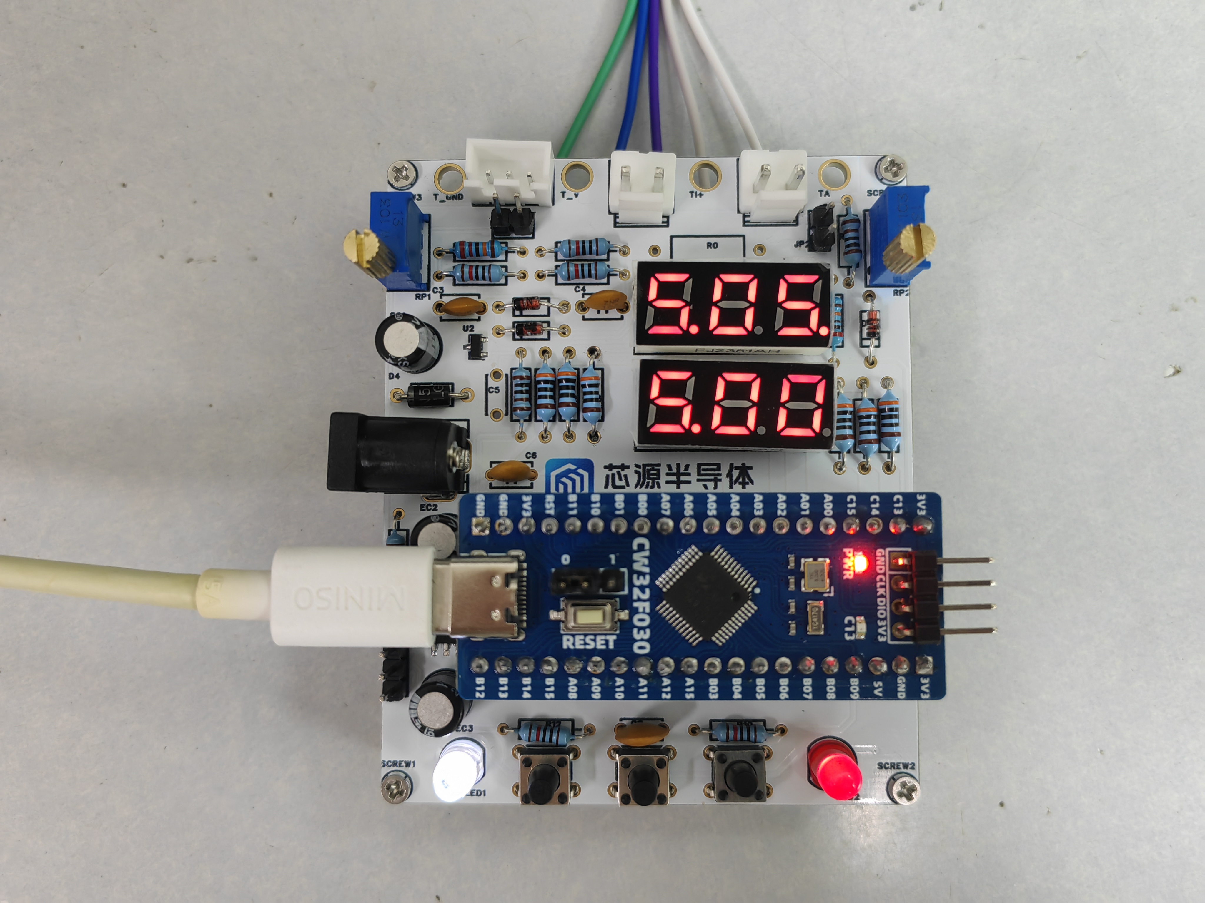
Mode 1: 5V voltage calibration setting, displays calibration number 5.05. After adjusting the measured bit to 5.00V, press the K2 key to calibrate the current value to 5V.
Mode 2: 15V voltage calibration setting, displays calibration number 5.15. After adjusting the measured bit to 15.0V, press the K2 key to calibrate the current value to 15V.
Mode 3: 0.5A current calibration setting, displays calibration number A.0.5. Press the K2 key to calibrate the current value to 0.5A.
Mode 4: 1.5A current calibration setting, displays calibration number A.1.5. Press the K2 key to calibrate the current value to 1.5A.
2.4 Timer Interrupt

The above code is a timer interrupt handler function BTIM1_IRQHandler(), used to handle the overflow interrupt of Timer 1. The following is a brief description of the timer interrupt handling function:
Each time a Timer 1 overflow interrupt occurs, first check if the overflow interrupt flag is set to ensure that the interrupt handling function is triggered by a Timer 1 overflow interrupt.
Perform the following main operations:
Obtain the ADC value using the Get_ADC_Value() function.
Control the LED to blink; after a certain time interval (ledcount greater than or equal to 1000), toggle the PC13 pin to achieve the LED blinking effect.
Update the runtime counter timecount.
Call the Dis_Refresh() function for scanning and displaying the digital tube.
Handle button operations:
Monitor button K1 (connected to pin 12 of GPIOB) to switch button modes.
Monitor button K2 (connected to pin 13 of GPIOB) and perform different processing based on the current mode:
Mode 1: Calibration voltage 5V.
Mode 2: Calibration voltage 15V.
Mode 3: Calibration current 0.5A.
Mode 4: Calibration current 1.5A.
The monitoring button K3 (connected to pin 13 of GPIOB) is used to return to mode 0, clear calibration data, and update the digital tube display.
This timer interrupt handling function implements the response to button operations, LED blinking control, digital tube display refresh, and voltage and current value calibration functions for different modes.
2.5 ADC Conversion

The above code is used to initialize the ADC. The following is a brief description of this function:
The ADC clock divider is set to 128, the reference voltage is selected as 1.5V, and the sampling time is set to 10 ADC clock cycles.
Channel ADC_SqrCh11, as the first channel of the ADC sequence (ADC_Sqr0Chmux), is connected to pin PB1.
Channel ADC_SqrCh9, as the second channel of the ADC sequence (ADC_Sqr1Chmux), is connected to pin PB0.
Channel ADC_SqrCh8, as the third channel of the ADC sequence (ADC_Sqr2Chmux), is connected to pin PB10.
Channel ADC_SqrCh12, as the fourth channel in the ADC sequence (ADC_Sqr3Chmux), is connected to pin PB11.
This configuration indicates that these four ADC channels (PB01, PB00, PB10, PB11) will be added to the ADC conversion sequence in a specific order and sampled in continuous conversion mode. This configuration allows the system to simultaneously and continuously acquire and convert the analog signals from these four channels to meet the system's needs for multiple analog signals.
III. Physical Demonstration
3.1 PCB


3.2 Panel and Housing

3.3 Overall Demonstration


CW32F030C8T6_Project.7z
PDF_Ammeter and Voltmeter.zip
Altium_current_voltmeter.zip
PADS_Ammeter and Voltage Meter.zip
BOM_CurrentVoltage Meter.xlsx
92858
LCSC CW32 Digital Voltage and Current Meter Expansion Board (Training Camp)
LCSC GeoStar CW32 Digital Voltage and Current Meter Expansion Board
I. Design Background
The digital voltmeter and ammeter combines ADC technology with circuit measurement principles, accurately converting analog voltage and current signals into digital displays for easy reading and analysis by electronic engineers. This device not only improves the accuracy and efficiency of circuit measurements but also helps engineers better understand circuit behavior, making it a powerful tool for electronic design and troubleshooting, and playing a significant supporting role in the work of electronic engineers. In product applications, the digital voltmeter and ammeter ensures the accuracy and safety of circuit design, while also providing strong support for product quality control and subsequent maintenance.
II. Hardware Design
Compared to the official case, this project has the following changes:
Power Supply Design :
This project uses the LDO chip 78L05 as the DC power output and the IP5306 as the battery management chip.
Voltage and Current Range Switching
: A jumper combined with a button is used for voltage and current range switching.
Display:
A 0.96-inch OLED display is used.
TrainingCampProjecct.zip
HnVideoEditor_2024_08_23_131342364_20240823_14221765.mp4
HnVideoEditor_2024_08_23_131342364_20240823_14221765_20240823_14280889.mp4
PDF_LCSC Diwenxing CW32 Digital Voltage and Current Meter Expansion Board (Training Camp).zip
Altium_LCSC·Diwenxing CW32 Digital Voltage and Current Meter Expansion Board (Training Camp).zip
PADS_LCSC CW32 Digital Voltage and Current Meter Expansion Board (Training Camp).zip
BOM_LCSC·Diwenxing CW32 Digital Voltage and Current Meter Expansion Board (Training Camp).xlsx
92859
CW32 Voltmeter and Ammeter Training Camp
LCSC GeoStar CW32 Digital Voltage and Current Meter Expansion Board
The hardware design
includes schematics,

PCB


layout, 3D shell panel, and software

design. The software is programmed using files from "Experiment 7 + Six-digit Current Channel Acquisition and Voltage Display.rar", "Experiment 8 + Simultaneous Voltage and Current Acquisition and Display.rar", and "Experiment 9 + Digital Voltage and Current Meter with Calibration Function.rar". The following images demonstrate the effects of "Experiment 7 + Six-digit Current Channel Acquisition and Voltage Display.rar" and "Experiment 9 + Digital Voltage and Current Meter with Calibration Function.rar". Note: If the following image appears when installing CW32F030_StandardPeripheralLib_V2.1.zipIdeSupportMDKWHXY.CW32F030_DFP.1.0.4.pack, rename the WHXY.CW32F030_DFP.1.0.4.pack file to WHXY.CW32F030_DFP.1.0.0.pack. The demonstration shows the effects of current channel acquisition and voltage display. Mode 1: Voltage 5V calibration setting; Mode 2: Voltage 15V calibration setting; Mode 3: Current 0.5A calibration setting; Mode 4: Current 1.5A calibration setting.


Schematic diagram.pdf
PCB.zip
Bill of Materials.xlsx
3D Shell.zip
panel.epanm
Experiment 7 + Six-digit display of current channel for voltage acquisition and display.rar
Experiment 8 + Simultaneous Acquisition and Display of Voltage and Current.rar
Experiment Nine + Digital Voltmeter and Ammeter with Calibration Function.rar
CW32F030_StandardPeripheralLib_V2.1.zip
PDF_CW32 Voltage and Current Meter Training Camp.zip
Altium_CW32 Voltmeter & Ammeter Training Camp.zip
PADS_CW32 Voltage and Current Meter Training Camp.zip
BOM_CW32 Voltage and Current Meter Training Camp.xlsx
92860
CW32 Voltage and Current Meter
This project is based on the LCSC CW32F030C8T6 development board and involves the design and implementation of a digital voltmeter and current meter. It covers hardware circuit design, firmware development, and related calibration and testing processes.
I. Project Function Introduction
The project's functions include:
Voltage Measurement: Accurately measures DC voltage and displays real-time voltage values.
Current Measurement: Accurately measures DC current and displays the current current value.
Calibration Function: Provides calibration interfaces and methods to ensure the accuracy of measurement results.
Physical Demonstration:

II. Hardware Design
1. MCU Selection: This project uses the LCSC CW32F030C8T6.
Key advantages of the CW32 in this project:
• Wide operating temperature range: -40~105℃
• Wide operating voltage range: 1.65V~5.5V (STM32 only supports 3.3V systems)
• Strong anti-interference: HBM ESD 8KV, all ESD reliability reaches the highest international standard level (STM32 ESD2K)
• Project focus - Better ADC: 12-bit high-speed ADC, achieving ±1.0LSB INL 11.3ENOB, multiple Vref reference voltages... (STM32 only supports VDD=Vref)
• Stable and reliable eFLASH technology.
2. Power Supply Circuit: The LDO selected is the SE8550K2, which can input a maximum voltage of 40V. However, for safety reasons, voltages exceeding 30V should be avoided. Alternatively, the Type-C interface or programming port on the development board can be used for power supply.

3. Voltage Sampling Circuit: Designed to sample voltages up to 100V, but for safety, the actual configuration is 0-30V. A voltage divider circuit is composed of 220KΩ and 10KΩ resistors, resulting in a voltage division ratio of 22:1. The ADC reference voltage in this project is 1.5V. A 1N4148 diode is used as a clamping diode to prevent damage to the MCU due to excessive input voltage. Diode clamping limits the voltage amplitude and protects the circuit from overvoltage damage. An additional voltage sampling circuit is added, selecting different sampling channels based on the actual voltage to improve measurement accuracy. Switching to a higher-precision channel is used within the 0-3V range for measurement.

4. Current Sampling Circuit: A low-side current sampling circuit is used for current detection. The low-side of the sampling circuit shares a common ground with the development board's meter interface. 5. Select a 100mΩ sampling resistor (be sure to choose a large package, such as 2512, or use a through-hole resistor) to detect a maximum current of 3A.


6. Voltage Measurement Calibration TL431 Circuit Design: An additional TL431 circuit is added to provide a 2.5V reference voltage, which can be used to provide an external voltage reference for the chip to calibrate the AD converter.

7. Digital Tube Display: Two 0.28-inch three-digit common-cathode digital tubes are used as display devices, with a 300Ω current-limiting resistor for the tubes.

8. LED Indicator: A power indicator and an LED connected to the microcontroller's PC13 port are added to the power supply circuit.

9. Button Circuit Design: Three buttons are provided for user use.

9. PCB Design:
Kelvin Connection of Current Sampling Resistor:

When placing the DC power interface and the pin header connecting the development board, pay attention to the placement position and distance (the center-to-center spacing of the pin headers connecting the development board is 600mil).

The DC power input should be placed sequentially according to the schematic diagram.


When using copper pour for the current sampling section, do not use the default divergent connection method with the pads; choose direct connection or use fill.

DRC Design Considerations:
Power traces should be as wide as possible, approximately 20-60mil.
Ordinary signal lines: around 10mil
. ADC signal traces: 10mil or 8mil. Too wide a trace may affect signal integrity when the line is too long.
III. Software Section
1. Concept of Calibration:
Calibration is the process of compensating for instrument system errors by measuring the deviation of a standard, thereby improving the accuracy and precision of the instrument or system. To improve the measurement accuracy and precision of voltage and current meters, calibration is required.
The common calibration principle is as follows:
Assume a sampling system where the AD part can obtain digital quantities, and the corresponding physical quantities are voltage (or current);
1. If an AD value point Xmin is calibrated at the "zero point" and an AD value point Xmax is calibrated at the "maximum point", according to the principle that "two points form a straight line", a straight line connecting the zero point and the maximum point can be obtained. The slope k of this line is easy to obtain. Then, by applying the equation of the straight line to solve for each point X (AD sample value), the physical quantity (voltage value) corresponding to the AD value can be obtained:

The slope k in the figure above:
k = (Ymax-Ymin)/(Xmax-Xmin)
(Because the first point is the "zero point", Ymin = 0 above)
Therefore, the physical quantity corresponding to the AD value at any point in the figure above:
y = k×(Xad-Xmin)+0
The above algorithm only calibrates between the "zero point" and the "maximum point". If the intermediate AD sample value is used, it will bring a large error in the corresponding physical quantity. The solution is to insert more calibration points.
As shown in the diagram below, four calibration points (x1, y1), (x2, y2), (x3, y3), and (x4, y4) are inserted.

This results in a line that is no longer a straight line but a "reflected line" (equivalent to segmented processing). To calculate the voltage value corresponding to a point Xad between x1 and x2:
y = k × (Xad – X1) + y1.
It can be seen that the more calibration points inserted, the higher the accuracy of the physical value.
When measuring voltage and current, a voltage and current calibration board or multimeter can be used to calibrate the collected voltage and current. The more calibration points, the more accurate the measurement.
2. Program Section:
The source program uses three calibration points. The voltage calibration points are 0V, 5V, and 15V. The current calibration points are 0A, 0.5A, and 1.5A. However, since I currently do not have power supply equipment above 15V, the voltage calibration points have been reset to 0V, 5V, and 10V. Therefore, the following programs are all written around these three values.
The main program code is as follows:

The calibration code calculation slope function is as follows:

The calibration storage function is as follows:

3. Burning Notes: When burning, you must select the correct programmer (select according to your own programmer).

IV. Calibration Settings
1. Five display modes and four calibration selections:
Mode 0: Displays normal voltage and current values (the upper row of digital tubes displays the voltage value *.V or .*V automatically switches, and the lower row displays the current value, _.**A).
Mode 1: 5V voltage calibration value setting. The upper row of digital tubes displays U.05. The lower row displays the current voltage value *.**V. In this mode, the multimeter should be used to measure the measured bit and adjusted to 5.00V. After pressing the K2 key, the current value is calibrated to the 5V voltage value.
Mode 2: 10V voltage calibration setting. The top row of the digital display shows U.10. The bottom row shows the current voltage value *.**V or **.*. In this mode, the multimeter should be set to 10.0V to measure the voltage being measured. Pressing the K2 key will calibrate the current value to 10V.
Mode 3: 0.5A current calibration setting. The top row of the digital display shows A.0.5. The bottom row shows the current current value *.**A. Pressing the K2 key will calibrate the current value to 0.5A.
Mode 4: 1.5A current calibration setting. The top row of the digital display shows A.1.5. The bottom row shows the current current value *.**A. Pressing the K2 key will calibrate the current value to 1.5A.
In modes 1-4, you can directly return to mode 0 by pressing button 3.
2. Voltage Calibration: (The calibration method for 5V and 10V is the same; two values need to be calibrated for accurate measurement.)
Use a DC power supply as the input and connect the jumper cap at JP1.
Connect the black probe of the multimeter to TGDND and the red probe to T_V.
Switch the mode to mode 1 using button 1.
Adjust RP1 until the multimeter displays 5.00V, then press button 2 to calibrate.
After calibration, press button 3 to return to mode 0.

3. Current Calibration: (The calibration method for 0.5A and 1.5A is the same; two values need to be calibrated for accurate measurement.)
Current calibration uses a voltage simulation method. The voltage displayed on the multimeter = R0 (0.1Ω) * actual current. Therefore, the voltage displayed on the multimeter * 10 can be considered the actual current value. (Do not solder R0 during calibration.)
Use a DC power supply as the input and connect the jumper cap at JP2.
Connect the black probe of the multimeter to TGDND and the red probe to TI+.
Switch to mode 3 using button 1.
Adjust RP2 until the multimeter displays 0.05V, then press button 2 to calibrate.
After calibration, return to mode 0 using button 3.

V. Appearance and Housing
1. JLCPCB Color PCB Design: The PCB design utilizes JLCPCB's color silkscreen printing process for a more attractive and aesthetically pleasing appearance.

2. JLCPCB Panel Design: The panel design is based on JLCPCB's technology and customized through the LCPCB online store. The panel uses a thin-film panel, which is highly transparent, blister-free, 0.2mm thick, and provides strong light shielding. The adhesive used is 3M9448A. It can be attached to a 3D housing.

3. 3D Housing Design: The housing was designed in SolidWorks and 3D printed by JLCPCB. The housing uses a top and back cover design, assembled with M3 screws and M3 nuts. (The screw length is 16mm)

Demonstration Video: [LCPCB Development Board] CW32 Voltage and Current Meter_Bilibili_bilibili
3D file.rar
Digital voltmeter and ammeter code.rar
BOM_V2.0_Schematic2_2024-08-21.xlsx
Demo video 50M.mp4
PDF_CW32 Voltage and Current Meter.zip
Altium_CW32 voltage and current meter.zip
PADS_CW32 Voltage and Current Meter.zip
92861
Ammeter used for learning based on the Geographic Star development board
Learning to build a digital voltmeter and ammeter is a good opportunity for beginners to gain a clear understanding of hardware and software. The digital voltmeter and ammeter project covers multiple aspects, including the design and implementation of microcontroller circuits, the design of signal acquisition and processing circuits, the development and optimization of the user interface, and the design of the product's appearance.
This project introduces
the creation of a digital voltmeter and ammeter, providing beginners with a clear understanding of hardware and software. The project covers various aspects, including microcontroller circuit design and implementation, signal acquisition and processing circuit design, user interface development and optimization, and product appearance design.
The project
provides voltage and current measurement functions, clearly displaying
the parameters
. Based on the JLCPCB Diwenxing development board, this voltmeter and ammeter design is very user-friendly for beginners. The integrated development board can independently implement the required functions, requiring only simple components and simple soldering. The hardware uses a DC power input port, supporting 5V~35V power input with a wide range and stable input. It uses a digital tube display, making it simple, safe, efficient, and durable. The Diwenxing development board is easy to use; simply write the code to use it. Other common components are also available, making replication cost-effective.
The software code is compiled using MK5. Related files are attached, along with a physical image.

Learning to use digital voltmeters and ammeters.rar
WeChat_20240823161102.mp4
WeChat_20240823161109.mp4
PDF_Ammeter for learning purposes using the Geographic Star development board.zip
Altium-based ammeter for learning purposes using the Earth Star development board. (zip file)
PADS_Ammeter for learning purposes using the Geographic Star development board.zip
BOM_Ammeter for Learning Based on the GeoStar Development Board.xlsx
92862
CW32 Voltage and Current Meter
The CW32 voltage and current meter I made in the LCSC training camp was basically based on the official case study. The only changes were replacing the resistors, capacitors, and other components with surface-mount 0603 packages and making some modifications to the wiring layout.
1. Project Function Introduction:
A voltage and current meter based on the CW32F030C8T6 chip
. 2. Project Attributes:
LCSC training camp project, for learning and familiarizing oneself with the CW32 chip from domestic Chipsource Semiconductor.
3. Open Source License
: GPL 3.0
4. Hardware Part:
The expansion board's appearance is shown in the image, using LCSC's color silkscreen printing.

The 3D shell is shown below; the top cover is open and has M2 screw holes, with recessed areas for the three buttons for easy operation. Because the shell itself is not very tall, there is no space reserved for the front panel.

One issue is the LED indicator lights. The placement of the two LED indicator lights wasn't considered much at the time of installation, and it was only after plugging in the CW32 that it was discovered that the CW32 board directly blocks these two LEDs, making them invisible from directly above, which is a bit awkward.

5. Software
: There's not much to say about the software; I didn't make any changes and directly used the official code. However, I encountered an error when using the official code directly. I'm not sure if it's a Keil version issue, but it couldn't recognize the WEAK decorator in cw32f030_systick.c, so I had to remove it.

Ultimately, I only tested the voltage measurement function because I didn't have suitable wires for the current connection port. I used DuPont wires to connect the voltage measurement port and tested its functionality as shown in the video.
Function demonstration.mp4
CW32gujian.zip
PDF_CW32 Voltage and Current Meter.zip
Altium_CW32 voltage and current meter.zip
PADS_CW32 Voltage and Current Meter.zip
BOM_CW32 Voltage and Current Meter.xlsx
92863
CW32-based voltage and current meters
A voltage and current meter based on CW32 was designed, and a 3D housing and panel were also designed.
Related Resources:
CW32 Digital Voltmeter and Ammeter Training Camp Project Tutorial Document | LCSC Development Board Technical Documentation Center
Explanation Video:
Step-by-Step Guide to Building a Voltmeter and Ammeter_bilibili
Physical Diagram


Hardware Design
1. Power Supply Circuit

LDO (Low Dropout Linear Regulator) Selection
This project uses an LDO as the power supply. Considering that most actual voltmeter products are used in industrial scenarios with 24V or 36V power supplies, this project selected the SE8550K2 with a maximum input voltage of up to 40V as the power supply. The main reason for not using a DC-DC step-down circuit to deal with the large voltage drop is to avoid introducing DC-DC ripple interference during the design process, and the secondary reason is to reduce project costs.
2. MCU Selection Analysis:
Key Advantages of CW32 in this Project
: Wide operating temperature range: -40~105℃;
Wide operating voltage: 1.65V~5.5V (STM32 only supports 3.3V systems)
; Strong anti-interference: HBM ESD 8KV; All ESD reliability reaches the highest international standard level (STM32 ESD 2KV);
Project Focus - Better ADC: 12-bit high-speed ADC, achieving ±1.0LSB INL 11.3ENOB; Multiple Vref reference voltages... (STM32 only supports VDD=Vref)
; Stable and reliable eFLASH technology.
A detailed explanation of these advantages will be provided in the chapters on ADC sampling and related extensions.
The main characteristics of the CW32 ADC:
This project focuses on the 4 reference voltage sources.
(Content from the "CW32x030 User Manual")

3. Voltage Sampling Circuit and Calibration Circuit:
The voltage divider resistors in this project are designed to be 220K+10K, therefore the voltage division ratio is 22:1 (ADC_IN11).

The calibration circuit is used to assist in the calibration of the voltage sampling circuit.

4. Current Sampling Circuit:
This project uses a low-side current sampling circuit for current detection. The low-side of the sampling circuit shares a common ground with the development board's meter interface
. Do not solder R17 during learning!

The calibration circuit is used to assist in the calibration of the current sampling circuit.
Do not solder resistor R17 during calibration!

5. Digital Tube Display:
This project uses a digital tube as the display device, specifically a 0.36-inch common cathode digital tube.

6. LED Indicators:
Power indicator,

user LED.

7. Button Circuit Design:
GPIO needs to be configured as pull-up input mode .

8. TL431 Circuit Design for Voltage Measurement and Calibration:
This project adds an extra TL431 circuit to provide a 2.5V reference voltage, which can be used to provide an external voltage reference for the chip to calibrate the AD converter.

Software Design
: 1. Using Systick as the main interrupt:
Based on Systick, an interrupt occurs every 1ms. All places requiring timed interrupts are placed in the Systick interrupt service function .
//cw32f030_systick.c
/**
* @brief This function handles System tick timer.
*/
void SysTick_Handler(void)
{
/* USER CODE BEGIN SysTick_IRQn */
uwTick += uwTickFreq;
Systick_Use();
/* USER CODE END SysTick_IRQn */
}
//main.c
/**
* @brief Called once every 1ms interrupt
*
*/
void Systick_Use()
{
if (++Adc_tc >= 1)
{
Adc_tc = 0;
Adc_ref = 1;
}
if (++Nixie_ref >= 2)
{
Nixie_ref = 0;
Nixie_Display();
}
if (++Key_tc >= 10)
{
Key_tc = 0;
Key_Loop();
}
if (++Nixie_cha_tc >= 300)
{
Nixie_cha_tc = 0;
Nixie_cha_ref = 1;
}
}
2. Button Function
K1: Switching Mode
Mode 0: Displays normal voltage and current values (the upper row of digital tubes displays the voltage value .V or .V automatically switches, the lower row displays the current value _ . ** A)
Mode 1: Voltage 5V calibration value setting. The upper row of digital tubes displays 5.05. The next row displays the current voltage value in .V or .V. In this mode, the multimeter should be set to 5.00V when measuring the measured position. Pressing the K2 key will calibrate the current value to 5V.
Mode 2: 15V voltage calibration setting. The upper row of the digital display shows 5.15. The next row displays the current voltage value in .V or .V. In this mode, the multimeter should be set to 15.0V when measuring the measured position. Pressing the K2 key will calibrate the current value to 15V.
Mode 3: 0.5A current calibration setting. The upper row of the digital display shows A.0.5. The next row displays the current current value in _.**A. Pressing the K2 key will calibrate the current value to 0.5A.
Mode 4: Current calibration value setting of 1.5A. The upper row of the digital tube displays A.1.5. The lower row displays the current current value *.** A. After pressing the K2 key, the current value is calibrated to 1.5A.
K2: Select to confirm the calibration value in non-mode 0 cases. K3
: Directly switch to mode 0.
3. Calibrate
5V

10V.
Because a 12V charger is used as the power source, it is not possible to calibrate 15V

0.5A

1A.

WeChat_20240823150404.mp4
CW32F030C8T6.zip
PDF_CW32-based voltage and current meter.zip
Altium_CW32-based voltage and current meter.zip
PADS_CW32-based Voltage and Current Meter.zip
BOM_CW32-based voltage and current meter.xlsx
92864
ammeter and voltmeter
LCSC GeoStar CW32 Digital Voltage and Current Meter
II. Hardware Design Details
Power Supply Circuit Design:
This project uses an LDO (Low Dropout Linear Regulator) as the power supply. Considering the actual application scenario, the SE8550K2 with a maximum input voltage of 40V was selected. A DC-DC step-down circuit was not used primarily to avoid potential ripple interference and to reduce costs.
MCU Selection Analysis:
This project uses the LCSC CW32F030C8Tx development board as the main controller. The selection considered computing power, I/O ports, and peripheral requirements. The CW32's advantages lie in its wide operating temperature range, wide operating voltage, strong anti-interference capability, and excellent ADC performance.
Voltage Sampling Circuit Design :
The voltage divider resistors are designed as 220K+10K, with a voltage division ratio of 22:1. Considering safety factors, the maximum measured voltage is designed to be 30V, but it can actually display 99.9V or 100V. The ADC reference voltage is 1.5V, which can be configured through the program. To reduce power consumption, the low-side resistor is selected as 10K. Calculations show that the high-side resistor is 220K. For measuring lower voltages, the voltage divider resistor can be replaced and the program modified to improve accuracy. For measuring higher voltages, the voltage reference can be increased to expand the range.
The current sampling circuit design
uses a low-side current sampling circuit with a designed sampling current of 3A and a sampling resistor of 100mΩ. Considering the voltage difference, power consumption, and amplification factor caused by the current sensing resistor, a 1W packaged metal wire-wound resistor was selected. To cope with different operating environments, especially high-current scenarios, the R0 resistor can be replaced with constantan wire or a shunt.
The digital tube display design
uses two 0.28-inch three-digit common-cathode digital tubes as display devices. Compared to a display screen, digital tubes have better recognition in complex environments and better mechanical performance. The current-limiting resistor is configured with 300Ω to achieve good display effect. The digital tube uses a dynamic scanning display driving method.
The LED indicator design
includes an additional power indicator and an IO working indicator. The power indicator LD_PWR is active low (on), and to reduce the current consumption of the LED, a 10K current-limiting resistor was selected.
The button
control circuit is designed to be simple, thanks to the CW32's internal I/O ports which can be configured with pull-up and pull-down resistors, eliminating the need for external configuration. One end of the button is connected to the MCU's I/O, and the other end is grounded. When the button is pressed, the I/O is pulled low. An additional
TL431
circuit is added to provide a 2.5V reference voltage, which can be used to provide an external voltage reference for calibrating the AD converter. The TL431 is a precision programmable reference device with high accuracy, adjustable output voltage, and a certain amount of current sinking capability. In this project, it is mainly used to learn the relevant application principles.
WeChat image_20240822151706.jpg
PDF_Ammeter and Voltmeter.zip
Altium_current_voltmeter.zip
PADS_Ammeter and Voltage Meter.zip
BOM_CurrentVoltage Meter.xlsx
92866
electronic


 京公网安备 11010802033920号

 STK14C88-C35


