1. The hardware design
is based on the official schematic but has been modified.
The digital display is replaced with an LCD1602.

A function to control relay voltage and current switching via buttons has been added.

4. Some modules have been removed.

5. A Type-C input has been added.

6. Most components are through-hole for easy soldering.
2. The software design
uses a timer to trigger ADC+DMA transfer.
`void AD_GPIO_Init(void)
{
__RCC_GPIOA_CLK_ENABLE(); // Enable GPIOA clock
__RCC_GPIOB_CLK_ENABLE(); // Enable GPIOB clock
PA00_ANALOG_ENABLE(); // Set PA0 as analog input
PA01_ANALOG_ENABLE(); // Set PA1 as analog input
PA01_ANALOG_ENABLE(); // Set PA2 as analog input
PB11_ANALOG_ENABLE(); // Set PB11 as analog input
}
// ADC configuration
void AD_Init(void)
{
__RCC_ADC_CLK_ENABLE(); // Enable ADC clock
ADC_DeInit();
ADC_SerialChTypeDef ADC_SerialChStruct; // ADC sequence configuration
ADC_SerialChStruct.ADC_SqrEns = ADC_SqrEns03; //` Convert SQR0, SQR1, SQR2, SQR3
ADC_SerialChStruct.ADC_InitStruct.ADC_OpMode = ADC_SerialChScanMode; // Sequence scan conversion mode
ADC_SerialChStruct.ADC_InitStruct.ADC_ClkDiv = ADC_Clk_Div128; // ADC clock frequency = PCLK / 4 = 64MHz / 4 = 16MHz
ADC_SerialChStruct.ADC_InitStruct.ADC_SampleTime = ADC_SampTime10Clk; // Sampling time -> 10 ADC clock cycles
ADC_SerialChStruct.ADC_InitStruct.ADC_VrefSel = ADC_Vref_VDDA; // VDDA reference voltage
ADC_SerialChStruct.ADC_InitStruct.ADC_InBufEn = ADC_BufDisable; // Disable the input buffer (follower) when no additional drive capability or gain is required.
`ADC_SerialChStruct.ADC_InitStruct.ADC_TsEn = ADC_TsDisable;` // Disable the built-in temperature sensor.
`ADC_SerialChStruct.ADC_InitStruct.ADC_DMAEn = ADC_DmaEnable;` // Trigger DMA transfer upon ADC conversion completion.
`ADC_SerialChStruct.ADC_InitStruct.ADC_Align = ADC_AlignRight;` // Right-align ADC conversion results.
`ADC_SerialChStruct.ADC_InitStruct.ADC_AccEn = ADC_AccDisable;` // Disable result accumulation; the result of each conversion will not be added to the previous result.
ADC_SerialChScanModeCfg(&ADC_SerialChStruct); // Configure ADC serial scan conversion mode
// Configure channel
CW_ADC->SQR_f.SQR0 = ADC_ExInputCH0; // PA0
CW_ADC->SQR_f.SQR1 = ADC_ExInputCH1; // PA1
CW_ADC->SQR_f.SQR2 = ADC_ExInputCH2; // PA2
CW_ADC->SQR_f.SQR3 = ADC_ExInputCH12; // PB11
ADC_ExtTrigCfg(ADC_TRIG_GTIM2, ENABLE); // Configure ADC external interrupt trigger source to trigger timer 2
}
// ADC DMA configuration
void AD_DMA_Init()
{
__RCC_DMA_CLK_ENABLE(); // Enable DMA clock
DMA_DeInit(CW_DMACHANNEL1);
DMA_InitTypeDef DMA_InitStruct; // DMA initialization structure
DMA_StructInit(&DMA_InitStruct); // Fill the DMA initialization structure with default parameters
DMA_InitStruct.DMA_Mode = DMA_MODE_BLOCK; // Trigger unlocked transfer using BLOCK
DMA_InitStruct.DMA_TransferWidth = DMA_TRANSFER_WIDTH_32BIT; // Data width is 12 bits
DMA_InitStruct.DMA_SrcInc = DMA_SrcAddress_Increase; // ADC peripheral address is fixed
DMA_InitStruct.DMA_DstInc = DMA_DstAddress_Increase; // The target address is automatically incremented.
DMA_InitStruct.DMA_TransferCnt = 4; // Number of transfers: 4
DMA_InitStruct.DMA_SrcAddress = (uint32_t)(&(CW_ADC->RESULT0)); // ADC data register address (source address)
DMA_InitStruct.DMA_DstAddress = (uint32_t)ADC_Value; // Target address
DMA_InitStruct.TrigMode = DMA_HardTrig; // Hardware trigger
DMA_InitStruct.HardTrigSource = DMA_HardTrig_ADC_TRANSCOMPLETE; // ADC as trigger source
DMA_Init(CW_DMACHANNEL1, &DMA_InitStruct); // Initialize DMA
NVIC_EnableIRQ(DMACH1_IRQn); // Enable NVIC
NVIC_SetPriority(DMACH1_IRQn, 0); // Set interrupt priority
DMA_ITConfig(CW_DMACHANNEL1, DMA_IT_TC, ENABLE); // Enable DMA transfer completion interrupt
DMA_ITConfig(CW_DMACHANNEL1, DMA_IT_TE, ENABLE); // Enable DMA transfer error interrupt
}
void Error_Handler(void)
{
while(1)
{
}
}
// DMA interrupt function
void DMACH1_IRQHandler(void)
{
if (DMA_GetITStatus(DMA_IT_TC1) == SET)
{
CW_DMA->CNT1_f.CNT = 4;
CW_DMA->CNT1_f.REPEAT = 1;
CW_DMACHANNEL1->SRCADDR = (uint32_t)(&(CW_ADC->RESULT0)); // Set source address
CW_DMACHANNEL1->DSTADDR = (uint32_t)ADC_Value; // Set the target address
DMA_Cmd(CW_DMACHANNEL1, ENABLE); // Enable DMA
DMA_ClearITPendingBit(DMA_IT_TC1);
}
if (DMA_GetITStatus(DMA_IT_TE1) == SET)
{
DMA_ClearITPendingBit(DMA_IT_TE1);
}
}
MultiButton is used.
MultiButton is a small, simple, and easy-to-use event-driven button driver module that can infinitely expand the number of buttons. The asynchronous callback processing of button events can simplify your program structure, remove redundant hard-coded button processing, and make your button business logic clearer.
The calibration method is not used at the moment. 3. Test
voltage test


and current test


code.7z
PDF_Simple Voltage and Current Meter.zip
Altium Simple Voltage and Current Meter.zip
PADS_Simple Voltage and Current Meter.zip
BOM_Simple Voltage and Current Meter.xlsx
92960
Digital voltage and current meter based on CW32F030C8T6 development board
In short, I'm open-sourcing an expansion board for voltage and current meters.
The digital voltmeter and ammeter based on the LCSC CW32F030C8T6 is finally finished!
Unlike ordinary multimeters, it has a calibration function. When the measurement is inaccurate, you can calibrate it. Press the user button 1 to enter the 5V calibration mode, which displays S.05.
At this time, plug in a voltmeter and turn the long-handled potentiometer to make the voltmeter display 5V. The blue text below shows the voltage that is not calibrated in the meter. If you have time, you can also calculate the error [winking emoji].
Then press the user button 2 to enter the 15V calibration mode, which displays S5.15. Turn the potentiometer to 15V and press the user button 2 again to complete the calibration. Similarly, you can also calibrate the current. Press the back button 1, which is user 3, to return to mode 0 and enter the measurement mode. This is its highlight.
Bilibili video link. I will post the Oshwhub open source and code in the comments section tomorrow.
This link is not the original version. This version adds two switches and Type-C power supply.
Below is the official documentation. If you don't want to read it, just close it.
I. Design Background
ADC (Analog-to-Digital) A converter (analog-to-digital converter) is an indispensable key component in electronic systems. It converts continuous analog signals into digital signals, enabling digital processing and analysis. ADCs play a crucial role in signal conversion, measurement and data acquisition, control system input, and communication and signal processing. Their widespread application promotes the intelligent and precise control of electronic equipment across various industries, and is one of the key factors driving modern technological progress.
Digital voltmeters and ammeters combine ADC technology with circuit measurement principles, accurately converting analog voltage and current signals into digital displays for easy reading and analysis by electronic engineers. This device not only improves the accuracy and efficiency of circuit measurements but also helps engineers better understand circuit behavior, making it a powerful tool for electronic design and troubleshooting, and playing a vital supporting role in the work of electronic engineers. In product applications, digital voltmeters ensure the accuracy and safety of circuit design, while also providing strong support for product quality control and subsequent maintenance.

Learning to design and build a digital voltmeter and ammeter is highly beneficial for improving one's professional skills. The digital voltmeter and ammeter project covers multiple aspects, including the design and implementation of microcontroller circuits, the design of signal acquisition and processing circuits, the development and optimization of user interfaces, and the design of product appearance. It integrates knowledge from multiple fields such as electronic technology, microcontroller programming, circuit design, and industrial design. Considering the learning pace and knowledge absorption capacity of beginners, we have specially launched this introductory-level digital voltmeter and ammeter project, which is very suitable for beginners in electronic technology and those who want to learn more about microcontroller applications. This project has the following highlights:
it adopts a core board plus expansion board design concept and uses plug-in device design, making learning simpler and exploration more in-depth;
the core board uses the domestic Wuhan Xinyuan Semiconductor CW32 as the main controller, while being compatible with other similar development boards; however, the CW32 has advantages.
The project is highly comprehensive and practical, and can be used as a desktop instrument after completion;
the project has rich learning materials, including circuit design teaching, PCB design, code programming learning, and the cultivation of engineers' debugging capabilities.
2.1. Software Development Overview
2.1.1. Essential Knowledge Points for Embedded Systems
Embedded software development, as an interdisciplinary field of computer science and electronic engineering, requires developers to have a series of professional knowledge and skills. Essential knowledge for CW32-based embedded software development includes the following:
Programming Languages:
Proficiency in C (C++) is crucial, as it's the most commonly used programming language in embedded systems due to its direct hardware access capabilities and high code execution efficiency.
Understanding of assembly language is necessary for writing low-level drivers, interrupt handlers, and high-performance code segments.
A basic understanding of other programming languages such as Python and Java is required for specific situations.
Familiarity with the CW32 standard library is essential.
Data Structures and Algorithms:
Familiarity with various data structures, such as arrays, linked lists, stacks, and queues, as well as common algorithms like sorting, searching, and recursion.
The ability to select appropriate data structures and algorithms based on the resource constraints of the embedded system is required.
Computer Architecture:
Understanding of processor architectures, such as ARM and x86, as well as instruction sets and memory management is essential.
Familiarity with the hardware components of embedded systems, such as microcontrollers, FPGAs, and DSPs, is required.
The ability to readily refer to the CW32 embedded chip's datasheet and user manual to understand the operating principles of required peripherals is also essential.
Embedded Operating Systems (In-depth Knowledge):
Master commonly used embedded operating systems such as μC/OS and FreeRTOS, and understand their kernel, process management, memory management, device management, and file system principles.
Be able to design and manage operating system tasks to meet the needs of specific applications.
Hardware Interfaces and Peripherals:
Be familiar with common hardware interfaces such as GPIO, serial ports, SPI, and I2C, and be able to write corresponding drivers.
Understand commonly used hardware devices in embedded systems, such as sensors, actuators, and communication modules, and be able to interact with them.
Development Tools and Environment:
Be proficient in using integrated development environments (IDEs) such as KEIL, IAR, and Visual Studio for software development and debugging.
Master the use of cross-compilers to compile programs that can run on target hardware on the development computer.
Be familiar with the use of debuggers, and be able to perform software breakpoint debugging, single-step execution, and variable viewing.
System Analysis and Design:
Be able to perform project requirements analysis and transform requirements into software functional requirements.
Master the principles and methods of software architecture design, and be able to design efficient and maintainable software systems.
Understanding the real-time requirements of embedded systems enables the design of software systems that meet these requirements.
Testing and Verification:
Mastering unit testing, integration testing, and system testing methods and techniques allows for comprehensive software testing to ensure the correctness and stability of software functions.
Understanding the reliability requirements of embedded systems enables reliability testing and verification of software. Only by fully mastering this knowledge and possessing continuous learning capabilities can one become an excellent embedded software developer.
2.1.2 Initial Preparation:
Development environment installation (MDK 5.33 recommended), DAPLINK downloader, firmware library. The firmware library can be downloaded from the official website: www.whxy.com. Common debuggers such as STLINK, DAPLINK, PWLINK, WCHLINK, JLINK, etc., that support Cortex-M are acceptable. The
remaining software code is in the attachment. The video also
emphasizes not making money by selling boards but taking the cultivation of Chinese engineers as its mission. I really like this slogan.
The video is a rough cut because OshWhub has a 50MB limit. For the full version, please visit Bilibili: 【〖LCSC Training Camp〗 Adjustable Voltmeter and Ammeter Training Camp - Showcase - Bilibili】 https://b23.tv/9LSiefE
ADC-CW32 WORKS.zip
Experiment Nine + Digital Voltmeter and Ammeter with Calibration Function.zip
VID_20240821171555.mp4
VID_20240821171742.mp4
PDF_Digital Voltage and Current Meter Based on CW32F030C8T6 Development Board.zip
Altium Digital Voltage and Current Meter Based on CW32F030C8T6 Development Board.zip
PADS Digital Voltage and Current Meter Based on CW32F030C8T6 Development Board.zip
BOM_Digital Voltage and Current Meter Based on CW32F030C8T6 Development Board.xlsx
92961
CW3 voltage and current meter
Thanks to JLCPCB and Sinyuan Semiconductor for organizing this event, which gave me a learning opportunity. It was my first time doing a project, and I had to learn everything from scratch. This experience helped me discover many problems; only after prototyping and assembling did I realize the panel size was incorrect and the casing was a bit small.
Hardware Design
1. Power Supply Circuit
: LDO (Low Dropout Linear Regulator) Selection.
This project uses an LDO as the power supply. Considering that most voltmeter products are used in industrial scenarios with 24V or 36V power supplies, the SE8550K2 with a maximum input voltage of up to 40V was selected. The main reason for not using a DC-DC step-down circuit to handle the large voltage drop is to avoid introducing DC-DC ripple interference during the design process; a secondary reason is to reduce project costs.
When designing the DC plug, attention should be paid to the inner diameter of the DC socket. Common types include DC 2.1 and DC 2.5; ensure that the power connector and DC socket are compatible.
2. ADC Sampling Circuit:
Advantages of CW32 in this Project
. Better ADC: 12-bit high-speed ADC, achieving ±1.0LSB INL 11.3ENOB, multiple Vref reference voltages... ... (STM32 only supports VDD=Vref).
Key characteristics of CW32's ADC.
3. Voltage Sampling Circuit
: The voltage divider resistors in this project are 220K+10K, therefore the voltage division ratio is 22:1 (ADC_IN11).
The voltage divider resistor selection
is designed to measure the maximum voltage. For safety reasons, this project uses 30V (the actual maximum display value can be 99.9V or 100V).
The ADC reference voltage is 1.5V in this project, and this reference voltage can be configured through the program.
To reduce the power consumption of the sampling circuit, the low-side resistor (R7) is usually chosen as 10K based on experience.
Then, the high-side resistance of the voltage divider resistor can be calculated using the above parameters.
The required voltage division ratio is calculated, i.e., the ADC reference voltage. The input voltage is designed; using known parameters, 1.5V/30V = 0.05 can be calculated.
The high-side resistance is calculated as the low-side resistance/voltage division ratio; using known parameters, 10K/0.05 = 200K can be calculated.
A standard resistor is selected: a resistor slightly higher than the calculated value of 200K is chosen. We usually choose E24 series resistors; therefore, in this project, 220K, which is greater than 200K and closest to the calculated value, is selected.
4. Current Sampling Circuit
The sampling current designed for this project is 3A, and the selected sampling resistor (R0) is 100mΩ.
The selection of the sampling resistor mainly needs to consider the following aspects:
the maximum value of the pre-designed measurement current;
the voltage difference caused by the 3A current sensing resistor in this project; and
the power consumption of the current sensing resistor, which is generally not recommended to exceed 0.5V. A suitable package should be selected based on this parameter. Considering the power consumption (temperature) issue under high current, a 1W packaged metal-wound resistor was selected
. The voltage amplification factor of the current sensing resistor: No operational amplifier was used in this project to build an amplification circuit, so the factor is 1. The
current sensing resistance value can then be calculated using the above parameters. Selection:
Since no amplification circuit was used in this project, a larger sampling resistor was needed to obtain a higher measured voltage for measurement.
Considering that a larger resistor would result in a larger voltage difference and higher power consumption, a larger resistor cannot be selected indiscriminately.
A 1W packaged resistor was selected in this project, corresponding to a power rise of 1W.
Based on the above data, a 100mΩ current sensing resistor was selected in this project. According to the formula, 3A * 100mΩ = 300mV, 900mW.
5. Digital Tube Display:
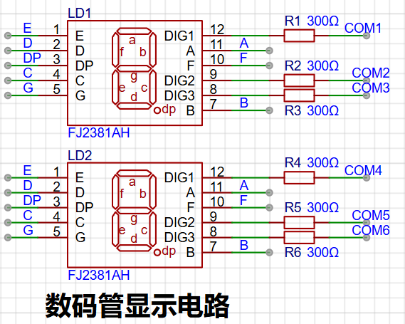
The driving principle of a digital tube mainly involves controlling the switching state of each LED segment to display numbers, letters, or symbols. The following is a detailed explanation of the driving principle:
Basic Structure of a Digital Tube:
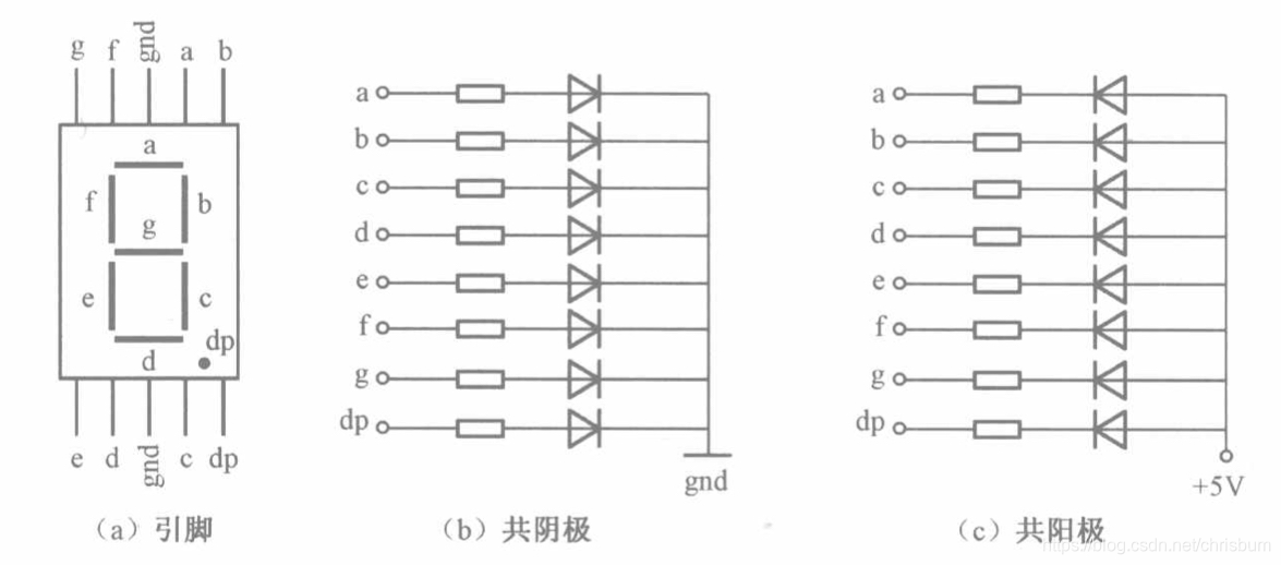
A digital tube typically consists of seven or eight LED segments (eight segments in this project). Each segment represents a part of the digital tube and can display numbers 0-9, letters AF, etc.
Digital tubes come in two types: common cathode and common anode. The difference lies in whether the common terminal COM (the end connecting all LEDs) is connected to the negative or positive terminal of the power supply.
Driving Methods:
Segment Selection: The desired number or character is displayed by controlling the switching state of each LED segment. Each segment corresponds to a control signal; when the control signal is on, the segment lights up, and vice versa. (a, b, c, d, e, f, g, dp)
Bit Selection: The digital tube to be displayed is selected by controlling the bit lines. Bit line control sets the bit line of the desired digital tube to a high level and the bit lines of other digital tubes to a low level. By continuously switching the state of the bit lines, the display switching between multiple digital tubes can be achieved.
Driving Circuit:
The digital tube driving circuit can be implemented through hardware circuits, such as using integrated circuits like digital signal processors (DSPs), microcontrollers (MCUs), or shift registers to generate control signals suitable for the LEDs.
These control signals can be in the form of pulse width modulation (PWM) signals, serial data signals, etc. By controlling the frequency, width, and amplitude of these signals, the brightness of the digital tube can be controlled, thereby displaying the desired numbers or letters.
Software Control:
In addition to hardware driving circuits, digital tubes can also be driven through software control. By programming to generate control signals suitable for the digital tubes, more flexible and complex display effects can be achieved, such as scrolling or alternating display of numbers.
Driving Common Cathode and Common Anode Digital Tubes:
For common cathode digital tubes, the common cathode pin is connected to the negative terminal of the power supply, and the control pin is connected to the output pin of the control chip. When a certain number needs to be displayed, the control chip outputs the corresponding encoded signal to the control pin, causing the corresponding LED segment to light up.
For common anode digital tubes, the working principle is similar to that of common cathode digital tubes, except that the common anode pin is connected to the positive terminal of the power supply, and the control pin is connected to the output pin of the control chip.
Encoding Display:
To display the corresponding numbers or characters on the digital tube, the segment data port must output the corresponding character encoding. For example, to display the number "0", the character encoding for a common anode digital tube is 11000000B (i.e., C0H), while the character encoding for a common cathode digital tube is 00111111B (i.e., 3FH). The specific encoding depends on the actual digital tube.
Dynamic and Static Display:
Digital tubes can use either static or dynamic display methods. In static display, each of the eight segments of each digital tube is connected to an 8-bit I/O port address. As long as the I/O port outputs a segment code, the corresponding character is displayed and remains unchanged. Dynamic display, on the other hand, lights up each digit of the digital tube one by one, achieving simultaneous visual display through rapid switching.
In summary, the driving principle of digital tubes is to control the switching state of each segment of the digital tube to display numbers, letters, or symbols, and to achieve display switching between multiple digital tubes through segment selection and digit selection. Furthermore, the driving of digital tubes can be implemented through hardware circuits or software control, and common cathode or common anode digital tubes can be selected for driving as needed.
This project actually uses dynamic scanning to drive the digital tube display.
Let's estimate the current required for the digital tube.
This project actually uses dynamic scanning to drive the digital tubes, so at any given time, only a maximum of 8 segments of the digital tubes (or LEDs) can be lit, or in other words, only one digit can be lit. According to the design, the required drive current is approximately 11mA (3.3V ÷ 300Ω ≈ 11mA) of the high-level voltage of the I/O port.
At this point, it's important to ensure that the selected MCU has sufficient current-source/current-sinking capability.
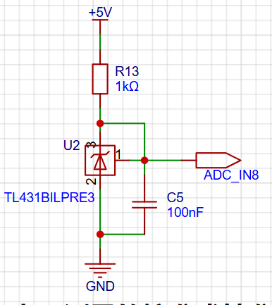
This project adds an extra TL431 circuit to provide a 2.5V reference voltage, which can be used to provide an external voltage reference for calibrating the AD converter. From a product design perspective, due to the inherent ADC performance advantages of the CW32, this circuit is not necessary. This circuit is designed on the development board to learn the relevant application principles.
The TL431 is a relatively "old" device, a classic, and widely used one, still found in many electronic products.
Many beginners may be encountering this device for the first time, so we will briefly explain its principles to help everyone better apply the TL431.
TI defines it as a "Precision Programmable Reference," and we can focus on several key characteristics on the first page of the references.
Precision: Precision indicates that its output voltage is very accurate. I used a TL431 with ±0.5% accuracy, which measured 2.495V on the board at room temperature. Compared to common Zener diodes, the accuracy is vastly different. In the application circuit diagram, the TL431 is represented by a Zener diode symbol.
Adjustable Output Voltage: The adjustable output voltage is between Vref and 36V. In our project, we use the output Vref voltage, which is approximately 2.5V. Therefore, we use 2.5V in the description, which is approximately equal to Vref.
Sinking Current Capability: This refers to how much current the output voltage pin can provide, which is greatly related to the resistance value (R13) in the application circuit. It should not be less than 1mA. If there is no need for sinking current, do not design the current to be too high, as this will cause unnecessary power consumption.
Digital voltmeter and ammeter with calibration function.zip
Panel_Panel_1_2024-08-21.epanm
CW32 voltmeter and ammeter housing. (zip)
test.jpg
Calibration Function.mp4
PDF_cw3 voltage and current meter.zip
Altium_cw3 voltage and current meter.zip
PADS_cw3 voltage and current meter.zip
BOM_cw3 Voltage and Current Meter.xlsx
92962
electronic


 京公网安备 11010802033920号

 75HQ045


