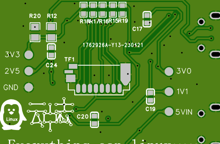
I. Schematic, PCB, BOM
A module for the OV2640 that can be used with OpenMV4 to adapt the FPC module to the OpenMV4 BTB socket.
The camera I'm using is https://m.tb.cn/h.gkDQKAOUux5XX3U?tk=fmPn3W9kW5P. M12 should be able to be screwed on.
The BTB connector I'm using is https://m.tb.cn/h.gkD9MfOiVl2YqBc?tk=uAQm3W9l4WF. I selected DF12NB(3.0)-36DP-0.5V.
The camera, in actual testing, requires flipping. An example is shown below:
```python3
import sensor
import time
sensor.reset() # Reset and initialize the sensor.
sensor.set_pixformat(sensor.RGB565) # Set pixel format to RGB565 (or GRAYSCALE)
sensor.set_framesize(sensor.QVGA) # Set frame size to QVGA (320x240)
sensor.set_hmirror(True)
sensor.set_vflip(True)
sensor.skip_frames(time=2000) # Wait for settings to take effect.
clock = time.clock() # Create a clock object to track the FPS.
while True:
clock.tick() # Update the FPS clock.
img = sensor.snapshot() # Take a picture and return the image.
print(clock.fps()) # Note: OpenMV Cam runs about half as fast when connected
# to the IDE. The FPS should increase once disconnected. The effect is shown in the image
;
frankly, it's not very good, and the frame rate isn't very high either. Just for fun.

PDF_CompatibleMV-OV2640.zip
Altium_CompatibleMV-OV2640.zip
PADS_CompatibleMV-OV2640.zip
BOM_CompatibleMV-OV2640.xlsx
93282
linux-card
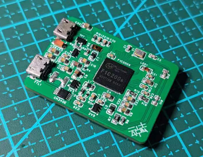
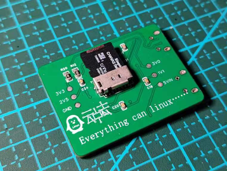
The first experimental board using the Allwinner F1C200S encountered many problems, but fortunately it eventually powered on successfully, and the Linux system was also successfully ported.
It's been a year and a half since the last sharing
of the Linux card machine project. The reason for the long delay in updating is mainly because the project has not made any substantial progress. Although we have done six PCB fabrications and modified the PCB repeatedly, the entire process has not been working. So, I will continue to update. Of course, this is also because my consistent principle is that any original content I share must be verified by myself as much as possible.
Fortunately, all the problems were perfectly resolved within the past week. The board was successfully driven, u-boot compiled and ran successfully, and Linux ran successfully, so I started updating again. First, let me show you the picture of the successful boot:
u-boot successfully driven
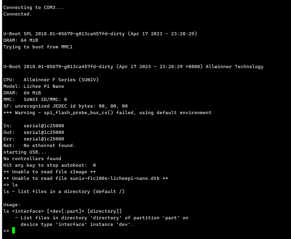
, Linux successfully running,

front and back
of the board.
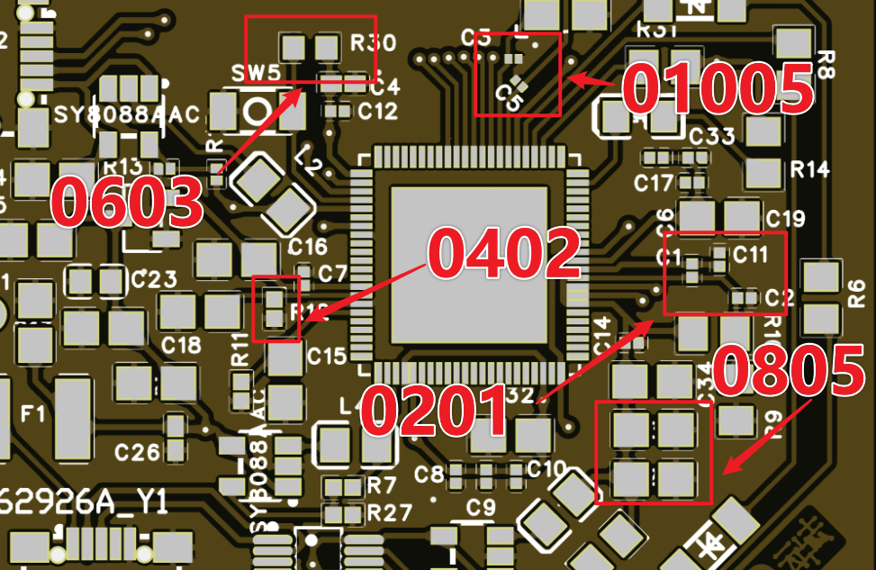
Today, I'll share my blood, sweat, and tears history of board making and designing. I made it 6 times, soldered it countless times, and stayed up countless nights... but it was worth it. The picture below shows the record of the six board making attempts, from top to bottom, from the first version to the sixth version. Although the sixth version still has some problems, it can run normally after jumpers and shorting. In

the first version
, I didn't even know what a package was. When designing the board, I involved all kinds of packages, including 0805, 0603, 0402, and even 01005 and 0201 packages. So the first board was basically impossible to solder. Of course, this is why the packages on the boards I have now are still a mess. After all, I can't waste the components I bought.
Second version... The third version
involved redrawing and fabricating the circuit board. After the second soldering, it was discovered that the chip pins were misaligned, causing a persistent short circuit. This led
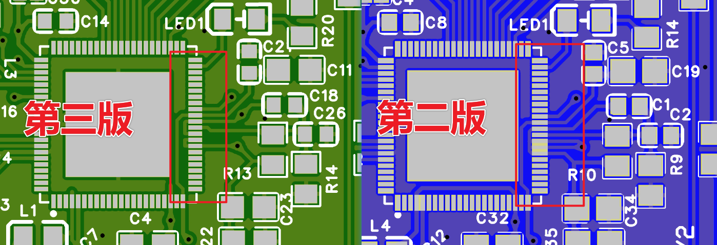
to the third version. Another change between the second and third versions was the removal of the LED from the serial port. I actually referenced another expert's schematic, who connected an LED instead of a light-emitting diode, suggesting a diode should be used. I drew a 1N4148 switching diode. Regardless of its rationality, drawing something haphazardly is definitely inappropriate. This serves as a reminder to anyone copying circuits: always understand the underlying principles before copying, or you'll only end up hurting yourself.
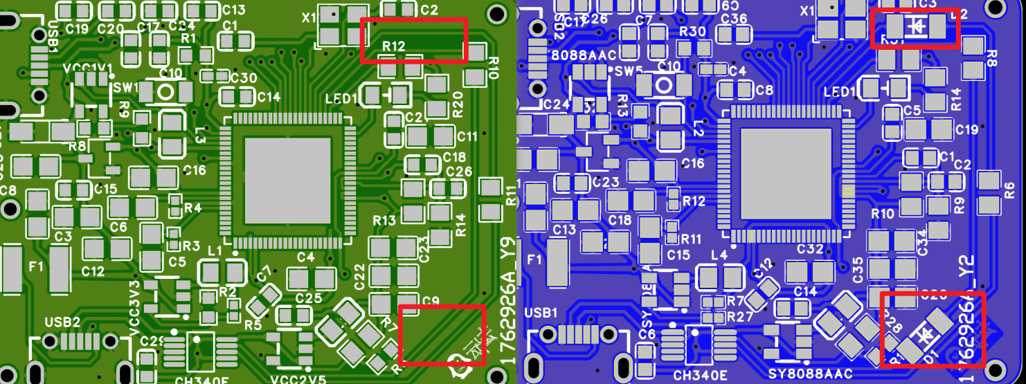
The third
version had an incompatible SD card slot, so a new board was made, since JLCPCB boards were readily available for free.

The fourth and fifth versions
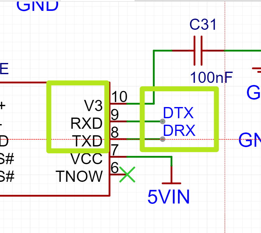
had the chip driving correctly, but the serial port would disconnect immediately upon pressing the reset switch. After comparison, it was discovered that the serial port connection was incorrect. I was using a CH340E chip, and RXD and TXD should correspond to the DTX and DRX of the F1C200S chip, respectively—reading corresponds to transmitting, and transmitting corresponds to reading. I hadn't known this before and drew it incorrectly, leading to this blunder.

The fifth version was then created. The fifth and
sixth versions were basically unchanged, except that because the serial port wasn't working, I referred to other people's schematics and added a 1uf filter capacitor to the reset pin.
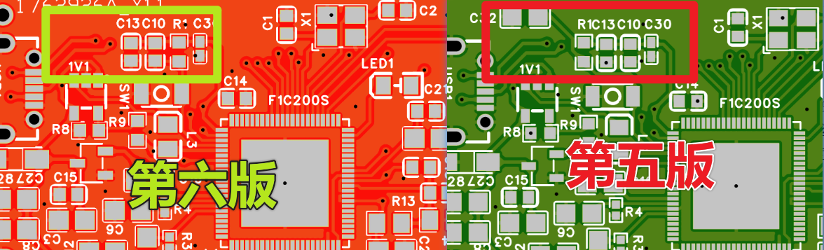
I also added some voltage test points.
However, just when I thought everything was finally over and I was about to power on this little board, fate played another trick on me.
PDF_linux-card.zip
Altium_linux-card.zip
PADS_linux-card.zip
BOM_linux-card.xlsx
93283
STC32G12K128-LQFP64 Core Edition - Serial Port Download
STC32G12K128-LQFP64 Core Design
1. Project Background
: With the rapid development of IoT, smart homes, industrial automation, and other fields, the demand for microcontrollers is increasing. The STC32G12K128-LQFP64, as a high-performance 32-bit microcontroller, has become the first choice for many developers and engineers due to its rich peripheral interfaces, powerful processing capabilities, and flexible programming environment. To meet the needs of rapid development and field debugging, implementing a stable and efficient serial port download program is particularly important.
Chip: STC32G12K128-LQFP64
Development Board: STC32G12K128-LQFP64 core board
Download Method: Onboard CH340N, downloading via serial port
2. Project Objectives
The core objective of this project is to achieve a comprehensive design of the STC32G12K128-LQFP64 core board, including hardware design, firmware programming, and the implementation of the serial communication protocol. The design aims to create a stable, efficient, and easy-to-use development platform to facilitate subsequent program development and debugging.
3. Design Concept
In the hardware design phase, we fully exposed all 64 pins of the STC32G12K128-LQFP64 chip, ensuring users can access and utilize every pin's
hardware connection: The STC32G12K128-LQFP64 core board has an onboard CH340N chip, which connects to a computer via a TYPE-C port for programming. ADC Module Design:
A precise
reference voltage design was provided for the chip's analog-to-digital converter (ADC) module, ensuring the ADC module can accurately acquire and convert analog signals. Power Supply Control:
The overall power supply of the development board is controlled via a toggle switch, allowing users to easily turn the power on or off for convenient power management.
FLASH Storage Circuit: A FLASH storage circuit is designed on the back of the development board, providing users with additional non-volatile storage space for convenient storage of programs and data.
Function Buttons: Three onboard function buttons, including a reset button, KEY1, and KEY2, provide users with convenient control methods for resetting the system, triggering specific functions, or performing user interactions.
Download Protocol: Briefly describe the download protocol or tools used, such as STC-ISP, STC-Flash, etc.
4. Test Results
Functional Test: Using STC-ISP for MCU detection, the MUC (STC32G12K128) was successfully detected.

5. Conclusion and Outlook
Conclusion: Through the implementation of this personal design project, I successfully completed the design and development of the STC32G12K128-LQFP64 core board. This process not only deepened my understanding of the characteristics of the STC32G12K128-LQFP64 chip but also improved my hardware design and firmware programming capabilities. The comprehensive pinout of the core board, the precise ADC module reference voltage design, the convenient power supply control switch, the rear FLASH storage circuit, and the integration of onboard function buttons together constitute a powerful and easy-to-use development platform.
During the project implementation, I encountered several technical challenges, such as power management stability and FLASH memory circuit compatibility. Through continuous learning and practice, I gradually overcame these challenges, which not only honed my problem-solving skills but also boosted my confidence. Through repeated testing and verification, I ensured the performance and stability of the core board, laying a solid foundation for subsequent program development and debugging.
The completion of this project marks my personal growth and progress in this field. I look forward to applying this core board to real-world projects to further verify its performance and optimize the design based on actual usage. At the same time, I hope to provide reference and assistance to other developers through this experience, jointly promoting technological development and innovation.
Overall, this personal design project is not only a process of technical practice but also a valuable experience in my career. I will continue to dedicate myself to learning and exploring the field of microcontrollers, constantly improving my technical skills to prepare for more complex and challenging projects in the future.
PDF_STC32G12K128-LQFP64 Core Version - Serial Port Download.zip
Altium_STC32G12K128-LQFP64 Core Edition - Serial Port Download.zip
PADS_STC32G12K128-LQFP64 Core Edition - Serial Port Download.zip
BOM_STC32G12K128-LQFP64 Core Edition - Serial Port Download.xlsx
93284
Intelligent Vehicle - DRV8701 Dual-Drive Open Source
DRV8701 Dual Drive, Compact Size
Schematic diagram:

The motor test is shown in the video; it can be used in both left and right directions, and also in reverse.
The DRV8701 can operate within a wide voltage range of 6-45V without external boost. One DRV8701E chip can drive multiple H-bridges.
The DRV8701E, in conjunction with an H-bridge circuit, is used to drive DC motors. Its working principle is to control the motor's speed (PWM) and direction (high and low levels) by controlling the input signal. It provides the current and voltage required for motor drive while protecting the motor from damage such as overcurrent, overvoltage, and short circuits. The DRV8701E also has several protection functions, such as overcurrent protection, overheat protection, and undervoltage protection, to ensure the safe operation of the motor and driver.
It can be used in intelligent car competitions (PCB layout modification required), electronic competitions, and other competitions for driving DC motors.
Advantages of this open-source project:
1. Small size.
2. Stable; it has been used for 1 year and 3 months and is still in use without damage. (No wiring errors, no damage, and no limit testing were performed during use).
3. The circuit can still work normally after the motor stalls.
4. The signal input section is isolated from the ground plane return current.
See the video for the principle:
https://www.bilibili.com/video/BV1SaYFeoE4Y/?spm_id_from=333.999.0.0
ccf123e96fbb012ad38e876e2bee0646.mp4
PDF_Intelligent Vehicle - DRV8701 Dual Drive Open Source.zip
Altium_Smart Car-DRV8701 Dual Drive Open Source.zip
PADS_Intelligent Vehicle-DRV8701 Dual Drive Open Source.zip
BOM_Intelligent Vehicle-DRV8701 Dual Drive Open Source.xlsx
93285
SimpleAMS
Homemade AMS (for bamboo terrariums)
Project Overview:
This project utilizes Topzhu's open MQTT interface, employing an ESP32 microcontroller to communicate with and send commands to the printer. Combined with supporting equipment, it achieves the color-changing effect of AMS.
The project consists of three main parts:
1. Control Board;
2. Supporting Bracket
; 3. Host Computer (Optional).
I. Control Board: The control
board is designed with two layers and extensively uses modules, making it simple to manufacture. Its interface functions are as follows.

II. Supporting Bracket:
The supporting bracket houses the extruder, motor, and servo motor, forming the hardware foundation for the color-changing function.

III. Host Computer (Optional)
: The host computer is written in WinForms, allowing for simple debugging and testing functions.

Project-related materials, including models and programs, are included in the attached compressed package.
Discussion Group QQ: 996068805.
Inspired by YBA-AMS.
SimpleAMS v1.0.rar
User Manual v1.0.pdf
PDF_SimpleAMS.zip
Altium_SimpleAMS.zip
PADS_SimpleAMS.zip
BOM_SimpleAMS.xlsx
93286
Miniature power solar booster
This is a solar lift module based on the LGS6302 chip, suitable for currents below 300mA. (This is a design by a novice circuit maker and may not meet standard specifications; the PCB is ported from a standard version and may have issues, so it's not recommended for reference.)
I. Project Introduction
A 2x2 5V solar panel system was used as the power source (two panels in series, then connected in parallel with two more panels in series)
. The first panel outputs 5V, 9V, and 12V.
Under midday sunlight, it outputs approximately 12V. At 5V output, the short-circuit current is approximately 300mA.
Input voltage:
![afac2293495f541940566a7932d94f8.jpg]

By changing the wiring caps, it can output approximately 5V, 9V, and 12V .
5V output:
![f607c46dcf43e569dd6888d63b5485c.jpg]

9V output: !
![51b8a3b40206a5d715157ed6353f238.jpg]

Second board: After connecting to the 5V output voltage of the first board (or external power supply), it is stepped down to 3.3V through LDO or charged to
3.3V through TP4056
![db3db3cf96695727c24bde5c672dbab.jpg]

Lithium battery charging (charging current set to 120mA)
Charging voltage is around 4V
![3ed7d9d4f850269fc6734f570988b91.jpg]

Charging indicator light
![e1e2d60efa1d6f8ab4c02dcfe066a45.jpg]

II. Precautions
1. Both boards are only used for voltages below 300mA. The first board's output voltage can be changed by adjusting the resistance ratio of R7, R6, R4, and R3 (refer to the chip datasheet for details). The second board's charging current can be changed by altering the resistance of R8 (the datasheet states that noticeable heat will occur when the current exceeds 0.5A).
2. The second board's PCB has a grounding DRC error; the 3.3V and charging modules are not grounded correctly. Ignore the DRC grounding error.
3. The solar panel should be used under sunlight; otherwise, the current will be too low, causing a voltage drop after connecting a load. The input voltage should be above 4V, with a certain voltage difference between it and the output voltage.
2. The board makes a sound when connected to a load, which may be due to improper selection of inductors and capacitors.
PDF_Minipower Solar Step-Up/Down.zip
Altium_Minipower Solar Buck-Boost.zip
PADS_Minipower Solar Buck-Boost.zip
BOM_Mini-Power Solar Step-Up/Down.xlsx
93291
electronic


 京公网安备 11010802033920号

 MI-P22-IXZ


