Design Task Analysis
: Design a generator capable of producing sine waves, square waves, triangle waves, and single-pulse signals, with the following requirements:
• Output frequency f: continuously adjustable from 20Hz to 5kHz for sine, square, and triangle waves.
• Output amplitude: 5V single-pulse signal.
• Output sine wave amplitude Vo: adjustable from 0 to 5V, with a waveform nonlinearity distortion coefficient y ≤ 5%.
• Output triangle wave amplitude Vo: adjustable from 0 to 5V.
• Output square wave amplitude: adjustable from 0 to 12V.
• Single-pulse output function. (
At the time, I wrote these to reach the word count.
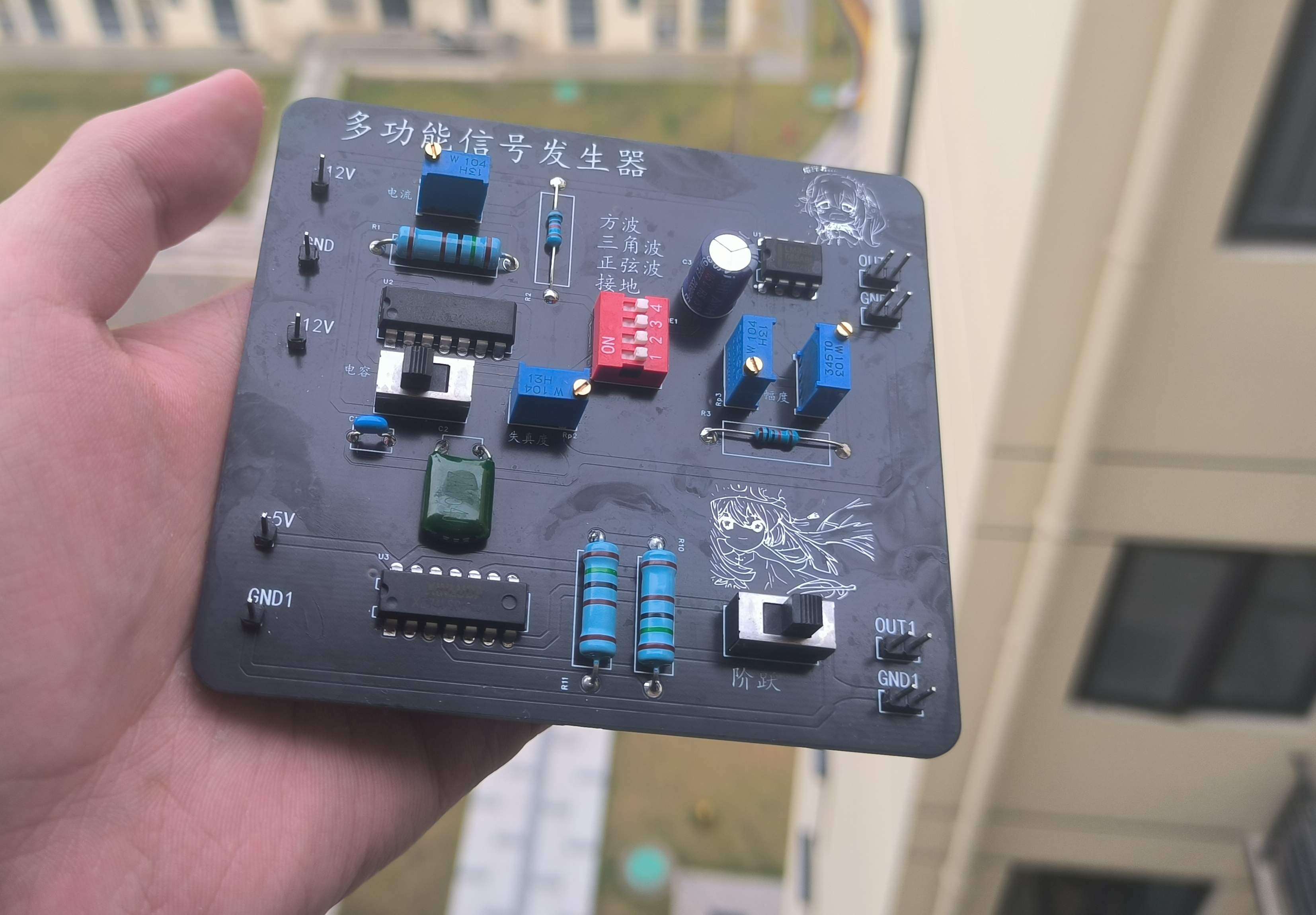
When I saw the course design requirements, my first reaction was to use a PCB. Considering the numerous and complex wires on a breadboard, it was better to use a more advanced method: wiring on a two-layer board.) Then came the schematic drawing. The reference schematic in the chip datasheet had some minor issues, such as resistor values, operational amplifier parameters, a missing negative power supply for the function chip, difficulty finding a single-pole triple-throw switch, and the absence of a step switch, etc. The above issues were addressed one by one during the schematic drawing process. This included correcting faulty lines, adjusting incorrect values, and replacing switches. After simulation, the schematic was confirmed to be error-free (especially the NAND gate section). Following this, the layout was moved to the next step. Considering the limited number of components, all were placed on a single side. The PCB was made larger, resulting in a neat, flat, and easy-to-operate layout. Considering the time-sensitive nature of PCBs, through-hole components were chosen. This facilitates soldering, and if a PCB isn't ready in time, a breadboard can be used as a lower-level replacement. This also helps the team understand the circuit. I prefer a more symmetrical layout, and considering the need for a layout close to the schematic for easier understanding, I made minor adjustments to the function section based on the schematic to maintain its aesthetic symmetry while keeping the relative positions of the smaller parts unchanged. For the step section, since the chip is a quad NAND gate integrated circuit, I simply connected the wires directly, then arranged the resistors and the replacement switches symmetrically horizontally. Then came the complex wiring. The main considerations are: on a single layer, lines must not overlap; using a double layer concentrates the lines, facilitating separate routing for the top and bottom layers; routing should be optimized to eliminate high-frequency signal interference; considering the characteristic of through-hole components connecting the top and bottom layers, unlike surface mount components, the routing must fully consider the top and bottom layers. Then there are considerations such as trace spacing and thickness. Finally, add appropriate and necessary silkscreen text instructions. Soldering through-hole components is relatively simple and will not be described in detail here. Although the overall layout is relatively open, attention should be paid to the soldering order in relatively concentrated areas to avoid component interference. Pay attention to soldering quality. Testing should proceed without problems.


 京公网安备 11010802033920号

 MA-161-054-447


