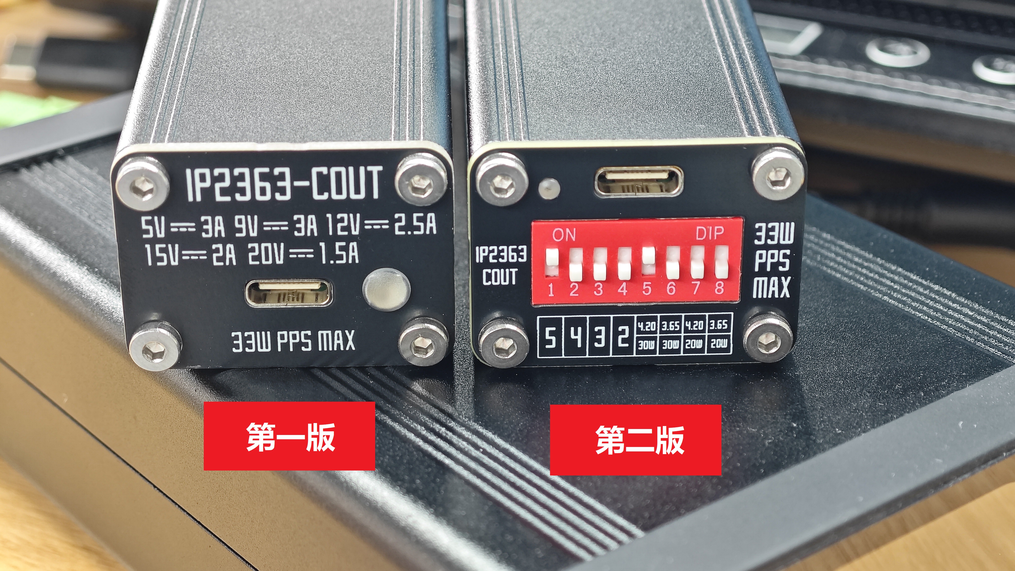
24.7.17 Update:
1. Added external DIP switches, updated to version 2, including 4 PCBs: the main board is 4 layers, and the DIP switch board and front and rear covers are 2 layers. You can use two coupons to complete an order by properly assembling the boards;
2. Upgraded the standard XT60 interface to an XT60 interface with a signal cable, and also brought out the NTC signal for easy use of NTC functions. Both types of XT60 connectors are compatible after the upgrade;
3. Reduced the size of the light guide column from 4mm to 2mm in diameter;
4. Reduced the hole diameter of the through-hole components on the main board and DIP switch board for precise positioning during manual soldering;
5. The schematic and PCB have been verified, and the BOM is correct. Please use with confidence. Additionally, JLCPCB has launched a new aluminum alloy shell design; the attached file is the completed 3D file of the charger shell design.
Precautions:
1. During installation, first install the motherboard and DIP switch board into the top and bottom covers respectively, then align the pin headers and sockets, and finally install the front and back covers and tighten the screws;
2. Due to firmware updates, some Xiaomi phones will not output when connected to Cout in a black screen situation. Output will only work normally after the screen is on, or by pressing the charger's touch switch in a black screen situation;
3. Reducing the sampling resistor value of the charging circuit can increase the charging current and the output current after Cout is induced, but the current connected to the phone will not change. A 0.5mΩ reduction in the sampling resistor value corresponds to an approximately 0.2A increase in current;
4. Solid capacitors on the motherboard should not exceed 10mm in height. If ultra-high height capacitors must be used, slots must be cut in the corresponding positions on the DIP switch board.
Update 24.7.9:
1. The slots for some aluminum profile housings had a negative tolerance, less than 32mm. The PCB width has been changed from 32mm to 31.8mm.
2. The diameter of the holes for solid capacitors and tactile switches has been changed from 1mm to 0.8mm for precise positioning and easier soldering.
I. Design Notes
1. Based on the existing project "IP2363 Verification Board", the PCB has been modified, and some component selections have been adjusted.
2. The DIP switch housing is internally designed and not exposed externally.
3. The USB-C and XT60 interfaces are designed to be flush with the front panel.
4. Please refer to another project for other design points.
5. The schematic and PCB are completely consistent with the actual product and have been verified. Please use them with confidence.
6. There is a space on the PCB where you can place a QR code. You can edit it according to your needs, for example, for DIP switch instructions.
7. Please refer to the attachment for the assembly BOM.
II. Test Data
1. Cout Output Efficiency

2. Charging Efficiency

3. Temperature Performance
(1) Cout Output: bare board, bare board + heat dissipation pad (with shell), bare board + heat dissipation pad (with shell) + heat dissipation aluminum sheet.

(2) Charging Input: bare board 3S charging, bare board 5S charging, 5S charging + heat dissipation pad (with shell) + heat dissipation aluminum sheet.

(3) Charging and discharging performance after installing the shell:

III. Summary
1. After adding the heat conduction pad, the temperature performance is consistent with that of the bare board after thermal equilibrium, but it can conduct the heat of the board to the shell more evenly;
2. Apply heat dissipation aluminum blocks to the chip and MOS tube to increase the heat dissipation area and reduce the peak temperature;
3. After installing the shell, the heat is concentrated in one half of the shell, and the peak temperature is below 50℃, which is lower than the human body's heat resistance limit of 60℃.
IV. Other
1. The positioning post of Port C needs to be cut off before soldering;
2. Inductors and MOSFETs can be reasonably replaced with other brands within the parameter range;
3. The light guide post is too large. If required, it can be changed to a smaller one. Be careful not to interfere with the side-emitting LED.


IP2363 Lithium Battery Charger Assembly List - V1.0.xls
IP2363 Lithium Battery Charger Assembly List - V2.0.xls
IP2363 battery charger aluminum alloy casing 3D file.stp
PDF_IP2363 Battery Charging Board.zip
Altium_IP2363 battery charging board.zip
PADS_IP2363 Battery Charging Board.zip
BOM_IP2363 Battery Charging Board.xlsx
93718
CH32V003-based keychain game console
A keychain game console based on CH32V003, offering a variety of mini-games.
This is a keychain game console based on the CH32V003, featuring several mini-games such as Galaga and Pac-Man.
This project is inspired by the CH32V003-GameConsole project by a foreign developer. The original project's PCB was quite large, so I redesigned it to fit as a keychain. [
https://github.com/wagiminator/CH32V003-GameConsole](https://github.com/wagiminator/CH32V003-GameConsole ) As usual, when making something yourself, you need a decent casing. The PCB, after extreme compression, is 24x40mm. With the battery, the overall casing, excluding the keychain ring, is 27mm wide, 42mm high, and 12mm thick. The front is less than the size of two coins.

Shell Model.zip
PDF_Keychain Game Console Based on CH32V003.zip
Altium_Keychain Game Console Based on CH32V003.zip
PADS_Keychain Game Console Based on CH32V003.zip
BOM_Keychain Game Console Based on CH32V003.xlsx
93719
Radar-sensing light painting with gravity sensor
Homemade radar-sensor light painting, the cheapest one online, costing only 10 yuan.
Preface to the Open Source Version of the Sensor Light Painting :
The previous version of the light painting used circuit boards cobbled together from a junk collector, resulting in incomplete functionality, poor display quality, and an inability to be fixed to a picture frame.
This revised version uses JLCPCB SMT circuit boards, consisting of 5 boards (19 RMB). Functional improvements include stepless touch dimming, the addition of yellow and white colors, a gravity switch for switching different light colors (single or dual selection), and the use of a TP4065 for battery charging.
Structural improvements include using a spring to hold the picture frame's built-in transparent PP cover, allowing direct replacement of the painting paper after pressing down the cover. See the video for specific usage. The final fixing uses a stapler to directly nail the circuit board to the wooden picture frame. If you don't have a stapler, you can use a stapler. The cost of the individual components can be found in my previous videos on Bilibili.
Introducing
the back and front USB lighting of the illuminated

LED display. Precautions for replacing the paper jam : 1. To save money on a few components, some resistor and capacitor values in the schematic are incorrect. This doesn't affect use, but the effect is not good. The resistor R8 between the stepless dimming chip and the touch pad is 5.1K. Changing the sensitivity adjustment capacitor C11 to 10nF can reduce sensitivity. Currently, 100nF is a bit too sensitive. Refer to the 6021WS chip manual for details. 2. It's best not to lay ground on the back and surrounding area of the touch pad connected to the 6021WS. 3. The 2K current-limiting resistor R3 can be removed and directly shorted. The sink current limit of SN74 is only tens of mA, which will limit the current. 4. The 2K current-limiting resistor R6 can be reduced as needed; otherwise, the light will not be bright enough. However, it cannot be shorted, otherwise it will burn out the LED. 5. Currently, the stepless dimming and radar sensing control two separate light paths. The output of the stepless dimming can be connected to the output of a photoresistor/AND gate for simultaneous control. See video for details. 6. Only one indicator light needs to be left on the TP4065. It's best to add a current-limiting resistor. Open-source link : LCSC Open Source Hardware Platform: https://oshwhub.com/fly_yang/radar_led_pcb Bilibili video: https://www.bilibili.com/video/BV164421D7L4/


Demo video.mp4
BOM_Board1_PCB1_2024-07-011.xlsx
Gerber_PCB1_2024-07-01.zip
PickAndPlace_PCB1_2024-07-01.xlsx
Stepless dimming 6021WS.pdf
TP4065.pdf
Logic gate SN74LVC1G00.pdf
Photosensitive.pdf
PDF_Radar-Sensing Light Image with Gravity Sensor.zip
Altium_Radar-Sensitive Lighting Picture with Gravity Sensor.zip
PADS_Radar-Sensitive Light Painting with Gravity Sensor.zip
BOM_Radar Sensor Lighting with Gravity Sensor.xlsx
93720
Development board based on STC32G12K128LQFP64
Based on the STC32G12K128LQFP64 development board, and referencing the official STC "Dragon Slayer III.2" guide, this version includes temperature measurement and flash expansion.
Participation is key. Coinciding with the STC & JLCPCB EDA☆2024 MCU Creative Design Competition, I planned to design a development board first, and coincidentally, the STC "Dragon Slayer Sword III.2" I requested also arrived. Inspired by the "Dragon Slayer Sword," I designed this development board. I happened to have a temperature sensing resistor on hand, so I added that as well. I'll skip the display part for now; STC's official debugging tool, STCAI-ISP, is very powerful and comes with a built-in virtual display.
1. Type-C16P power supply for downloading. CC1 and CC2 are grounded through a 5.1kΩ resistor, and PD induces 5V. Since this chip supports direct USB downloading, a CH340 is not needed, so UD+ and UD- are directly connected to the chip's P3.0 and P3.1 pins through a 30Ω resistor.

2. Downloading requires P3.2 to be grounded before powering on to enter download mode. Therefore, the power supply circuit is controlled by a transistor. The original design used a B1204, but it wouldn't fit on my board. I chose the SS8550; the 1.5A collector current seems sufficient, but the 300mW power consumption is unclear. I assumed it was the transistor's own power dissipation, but I'm not sure if that's correct. It's likely to fail. I've reserved pads on the bottom of the PCB as a precaution.
The power is off when the button is pressed and restored when released. I'm using an LDO to convert 5V to 3.3V.

3. This chip has a wide voltage range of 1.9V-5.5V. Considering the external power supply circuit, VCC can be selected as 3.3V or 5V via a jumper.

4. The chip has a reference voltage; I'm not sure if it's necessary. I noticed the temperature resistor also needs a reference voltage, so I'm adding that as well.

5. I'm adding flash memory expansion for practice.

6. I'm used to including indicator lights in every design. This allows me to check if the chip's power supply is normal and if the program is being copied correctly.

7. The main control chip requires capacitors. When routing, keep them as close to the chip pins as possible.

8. The main control chip's circuit diagram and package are too large to include here. 9. Pinouts are arranged
exactly as described in Section 3.2 of the "Dragon Slayer Sword" guide.
10. Check DRC (Digital Control Code), extremely important!!!
11. Dimensions: 84mm*33mm, meeting JLCPCB's free conditions.
12. 3D diagram. 13. PCB fabrication: First time doing color silkscreen printing, the color scheme is terrible, but please bear with it. 14. Soldering . 15. Power on . 16. Open STC-ISP software, select the microcontroller model, leave other settings as default, press and hold the P3.2 dropdown button, then press the circuit restart button. The software automatically detects the serial port, opens the program file, and downloads the program. 17. Ignite the LEDs: The two LEDs are different brightness levels because one was soldered incorrectly, so I just used a random 0805. I found that the 0603 pad is practically universal; 0805 and 0402 components can be used as substitutes. There's only one 0402 resistor on the board. 18. Temperature: Cannot demonstrate, spent two days working on Keil software without success. I'll submit my assignment now.


WeChat_20240716162505.mp4
PDF_Development board based on STC32G12K128LQFP64.zip
Altium development board based on STC32G12K128LQFP64.zip
PADS_Development Board Based on STC32G12K128LQFP64.zip
BOM_Development Board Based on STC32G12K128LQFP64.xlsx
93721
AIR32_DAP
DAPlink V2
This is a modified version of the DAPlinkV2 schematic from DAPlink
, and it can directly use DAPlink's firmware.
It
supports connection using header pins and 1mm*8 cables; it's small and cute.

air32_daplink_v2.hex
test.7z
PDF_AIR32_DAP.zip
Altium_AIR32_DAP.zip
PADS_AIR32_DAP.zip
BOM_AIR32_DAP.xlsx
93723
Fast-edge pulse square wave generator
A fast-edge pulse square wave generator produces a square wave signal with a fast edge.
This fast-edge pulse square wave generator produces a square wave signal with a fast edge. It can be used in scenarios requiring low-cost generation of fast rise/fall times.
The measured rise time of this circuit is less than 600ps. According to the formula BW=0.35/Tr, it can also be used to test
how the frequency of the generated waveform can be changed by modifying the values of R9 and C6.
Introductory video: [Fast-edge pulse square wave generator, oscilloscope bandwidth testing, signal reflection testing]
PDF_Fast Edge Pulse Square Wave Generator.zip
Altium_Fast-Edge Pulse Square Wave Generator.zip
PADS_Fast Edge Pulse Square Wave Generator.zip
BOM_Fast Edge Pulse Square Wave Generator.xlsx
93725
FPGA-EP4CE6E22+ESP32
The FPGA and ESP32 were designed on the same circuit board.
Chip Model
: FPGA: EP4CE22E22C8N ;
ESP32: ESP32-12F . The FPGA has as many pins as possible for easy secondary development. The FPGA is connected to the ESP32's serial port. Packaging and Soldering : The FPGA is in an LQFP package, and all resistors and capacitors use 0805 or larger packages for easy DIY manual soldering. Circuit Board Design: This circuit board was designed using LCSC EDA Professional Edition. It is a four-layer board with a power supply range of 5.5-36V.
PDF_FPGA-EP4CE6E22+ESP32.zip
Altium_FPGA-EP4CE6E22+ESP32.zip
PADS_FPGA-EP4CE6E22+ESP32.zip
BOM_FPGA-EP4CE6E22+ESP32.xlsx
93726
STC32G12K128-LQFP48 Development Board
The simple STC32G128K development board measures approximately 49.4mm x 72mm.
The main controller uses an STC32G12K128-35I-LQFP48
with 33 I/O ports. It has an onboard
5V to 3.3V
converter, one onboard power LED, one
onboard user LED, two onboard user buttons, one power switch, an external
8MB
FLASH interface, an onboard thermistor, a DS18B20
onboard satellite positioning module,

and Figure 1 (front view),

Figure 2 (back view), and

Figure 3 (power-on effect).
PDF_STC32G12K128-LQFP48 development board.zip
Altium_STC32G12K128-LQFP48 development board.zip
PADS_STC32G12K128-LQFP48 development board.zip
BOM_STC32G12K128-LQFP48 Development Board.xlsx
93727
#Bootcamp# Simple Oscilloscope Based on GD32 -- 5589055A
GD32-based oscilloscope
(1) Analog front-end processing circuit: responsible for processing the input detection analog signal and then giving it to the microcontroller for recognition. The specific circuit includes AC/DC coupling selection circuit, voltage attenuation circuit, and signal processing circuit.
(2) Power supply circuit: using the LCSC GD32E230C8T6 development board to convert 5V to 3.3V via LDO.
(3) Microcontroller part: directly using the LCSC GD32E230C8T6 development board to connect to the motherboard via a header.
(4) Human-machine interaction circuit: used to control the oscilloscope functions, including buttons, encoder, 1.8-inch TFT LCD screen, providing a foundation for the development of oscilloscope functions.
Measurement range: -80V — +250V.
Refer to the official case.
The oscilloscope can automatically capture the waveform, frequency, phase, etc. of the signal and present them on the display screen
to facilitate the analysis of the circuit working status.
PDF_#Training Camp# Simple Oscilloscope Based on GD32--5589055A.zip
Altium_#Training Camp# Simple Oscilloscope Based on GD32 -- 5589055A.zip
PADS_#Training Camp# Simple Oscilloscope Based on GD32 -- 5589055A.zip
BOM_#Training Camp# Simple Oscilloscope Based on GD32 -- 5589055A.xlsx
93728
electronic


 京公网安备 11010802033920号

 Am29LV102BB-90JC


