Why do we need a gate driver? What are the key parameters of a gate driver?
Source: InternetPublisher:aerobotics Keywords: MOSFET Driver Gate Driver Updated: 2025/02/28
Why do we need a gate driver?
The structure of the IGBT/power MOSFET is such that the gate forms a non-linear capacitor. Charging the gate capacitance turns the power device on and allows current to flow between its drain and source pins, while discharging turns the device off and large voltages can be blocked across the drain and source pins.
The minimum voltage at which the gate capacitance is charged and the device is just ready to turn on is the threshold voltage (VTH). To use an IGBT/Power MOSFET as a switch, a
voltage sufficiently greater than VTH should be applied between the gate and source/emitter pins.
Consider a digital logic system with a microcontroller that can output a 0 V to 5
V PWM signal on one of its I/O pins. This PWM will not be sufficient to fully turn on the power devices used in the power system because their overdrive voltages typically exceed standard CMOS/TTL logic voltages.
Therefore, an interface is required between the logic/control circuitry and the high power device. This can be achieved by driving a logic level n-channel MOSFET, which in turn drives a power MOSFET, as shown in Figure 1a.
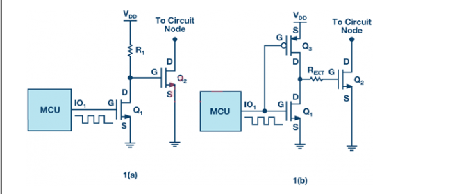
Figure 1. Driving a power MOSFET with inverting logic.
As shown in Figure 1a, when IO1 sends a low signal, VGSQ1 < VTHQ1, so MOSFET Q1 remains off. As a result, a positive voltage is applied to
the gate of power MOSFET Q2. The gate capacitance (CGQ2) of Q2 is charged through the pull-up resistor R1, and the gate voltage is pulled to the rail voltage of VDD.
If VDD > VTHQ2, Q2 is on and can conduct current. When IO1 outputs a high level, Q1 is on and CGQ2 discharges through Q1. VDSQ1 ~ 0 V makes VGSQ2
< VTHQ2, so Q2 is off. One problem with this setup is the power dissipation in R1 when Q1 is on.
To solve this problem, pMOSFET
Q3 can be used as a pull-up device, which works in a complementary manner to Q1, as shown in Figure 1b. PMOS has a low on-resistance and a very high off-resistance, and the power consumption in the drive circuit is greatly reduced. To control the edge rate during the gate transition,
a small resistor is added between the drain of Q1 and the gate of Q2.
Another advantage of using MOSFETs is that they are easy to make on die, whereas resistors are relatively difficult to make. This unique interface for driving the gate of a power switch can be created in the form of a monolithic IC that accepts a logic level voltage and produces a higher power output. This gate driver IC will almost always have other internal circuitry to achieve more functionality, but it is primarily used as a power amplifier and level shifter.
Key parameters of gate drivers
Drive Strength
The problem of providing the proper gate voltage is solved by the gate driver, which performs the level shifting task. However, the gate capacitor cannot change its voltage instantaneously. Therefore, the power FET or IGBT has a non-zero finite switching interval time.
During switching, the device may be in a high current and high voltage state, which generates power dissipation and turns into heat. Therefore, the transition from one state to another needs to be fast to minimize the switching time. To achieve this, high transient currents are required to quickly charge and discharge the gate capacitance.
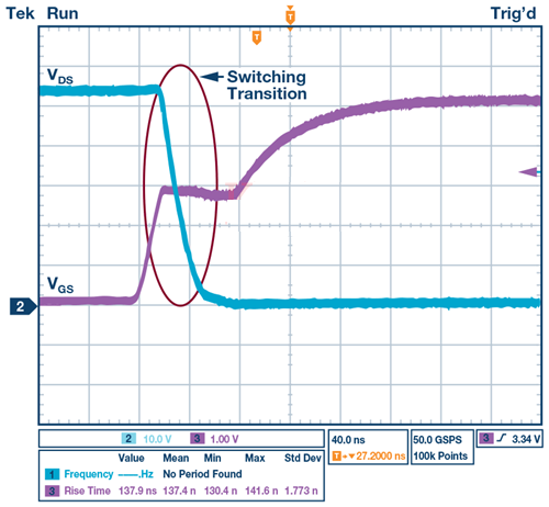
Figure 2. MOSFET conduction transition without gate driver
Drivers that can source/sink higher gate currents for longer periods of time will have faster switching times and, therefore, lower switching power dissipation in the transistors they drive.
Microcontroller I/O pins are typically rated for sourcing and sinking currents up to tens of milliamps, while gate drivers can deliver much higher currents. In Figure 2, a long switching interval is observed when the power MOSFET is driven by a microcontroller I/O pin at its maximum rated source current.
As shown in Figure 3, the transition time is greatly reduced when using the ADuM4121 isolated gate driver, which is capable of providing much higher drive current than a microcontroller I/O pin when driving the same power MOSFET.
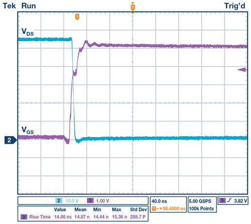
Figure 3. MOSFET conduction transition with gate driver
In many cases, driving a larger power MOSFET/IGBT directly with a microcontroller may cause the controller to overheat and be damaged because the digital circuit may overdraw current. Gate drivers have higher drive capabilities and support fast switching, with rise and fall times of only a few nanoseconds. This can reduce switching power losses and improve system efficiency. Therefore, drive current is often considered an important indicator for selecting gate drivers.
Corresponding to the drive current rating is the gate driver’s drain-source on-resistance (RDS(ON)). Ideally, the RDS(ON) value when the MOSFET is fully on should be zero, but due to its physical structure, this resistance is generally in the range of several ohms. This takes into account the total series resistance in the current path from drain to source.
RDS(ON) is the true basis for the maximum drive strength rating of a gate driver, as it limits the gate current that the driver can provide. The RDS(ON) of the internal switch
determines the sink and source current, but the external series resistor is used to reduce the drive current and therefore affects the edge rate.
As shown in FIG4 , the high-side on-resistance and the external series resistor EXT constitute the gate resistor in the charging path, and the low-side on-resistance and REXT constitute the gate resistor in the discharging path.
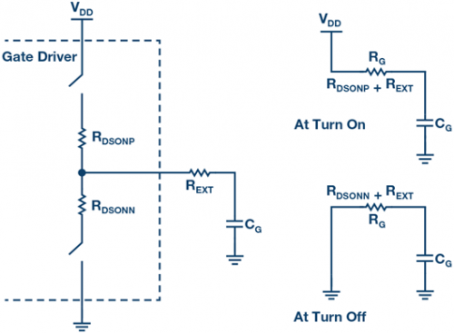
Figure 4. RC circuit model of a gate driver with a MOSFET output stage and the power device acting as a capacitor
RDS(ON)
also directly affects the power consumption inside the driver. For a specific drive current, the lower the RDS(ON) value, the higher the REXT value that can be used. The power consumption is distributed between REXT and RDS(ON), so a higher REXT value means more power consumption outside the driver.
Therefore, for a given chip area and size of the IC, the lower the RDS(ON) value, the better in order to improve system efficiency and relax thermal regulation requirements within the driver.
Timing
Gate driver timing parameters are critical to evaluating their performance. A common timing specification for all gate drivers, including the ADuM4120 (shown in Figure 5), is the driver’s propagation delay (tD)
, which is defined as the time required for an input edge to propagate to the output.
As shown in Figure 5, rising propagation delay (tDHL) can be defined as the time from the input edge rising above the input high threshold (VIH) to the time the output rises to more than 10% of its final value.
Similarly, the falling propagation delay (tDHL) can be stated as the time from the input edge falling below the input low threshold, VIL, to the time the output falls below 90% of its high level. The propagation delay for the output transition can be different for rising and falling edges.
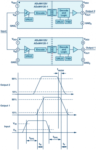
Figure 5. ADuM4120 gate driver and timing waveforms
Figure 5 also shows the rise and fall times of the signal. These edge rates are affected by the drive current that the device can provide, but they also depend on the load being driven, which is not accounted for in the propagation delay calculation.
Another timing parameter is pulse width distortion, which is the difference between the rising and falling propagation delays of the same device. Therefore, pulse width distortion (PWD) = |tDLH – tDHL|.
Due to transistor mismatches within different devices, the propagation delays of two devices will not be exactly the same. This results in propagation delay skew (tSKEW), which is defined as the time difference between the output transitions of two different devices in response to the same input under the same operating conditions.
Propagation delay skew is defined as part-to-part variation, as shown in Figure 5. For devices with multiple output channels, this specification is stated the same way, but is referred to as channel-to-channel skew. Propagation delay skew cannot usually be compensated in the control circuitry.
Figure 6 shows a typical setup of the ADuM4121 gate driver, used in conjunction with power MOSFETs in a half-bridge configuration for power and motor drive applications. In this setup, if Q1 and
Q2 are turned on at the same time, there is a chance that shoot-through will occur due to the shorting of the power and ground pins. This can permanently damage the switches and even the driving circuitry. To avoid shoot-through, a dead time must be inserted into the system to greatly reduce the probability of both switches being turned on at the same time.
During the dead time interval, the gate signals of both switches are low, so ideally the switches are in the off state. If the propagation delay skew is low, then the required dead time is shorter and the control becomes more predictable. The lower the skew and the shorter the dead time, the smoother and more efficient the system operation.
Timing characteristics are important because they affect the speed at which the power switches can operate. Understanding these parameters can make control circuit design simpler and more accurate.
isolation
Isolation refers to the electrical separation between the various functional circuits in a system so that there is no direct conductive path between them. This allows different circuits to have different ground potentials. Signals and/or power can still pass between isolated circuits using inductive, capacitive or optical methods.
For systems using gate drivers, isolation may be necessary to perform the function and may also be a safety requirement. In Figure 6, VBUS may be several hundred volts and tens of amps may be flowing through Q1 or
Q2 at any given time.
In the event of a fault in this system, if the damage is limited to the electronic components, safety isolation may not be necessary, but if human activity is involved on the control side, galvanic isolation is required between the high power side and the low voltage control circuits. It protects against any fault on the high voltage side, as the isolation barrier will prevent power from reaching the user despite component damage or failure.
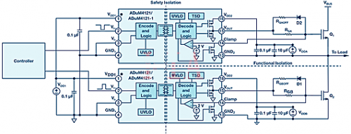
Figure 6. Isolation barrier in a half-bridge setup using the ADuM4121 isolated gate driver.
Isolation is a mandatory requirement by regulatory agencies and safety certification bodies to prevent the risk of electric shock. It also protects the low voltage electronics from any damage caused by faults on the high power side. There are many ways to describe safety isolation, but at a basic level, they all relate to the breakdown voltage of the isolation barrier.
This voltage rating is generally given for the lifetime of the driver and for voltage transients during specific periods and situations. These voltage levels are also related to the physical size of the driver IC and the minimum distance between pins across the isolation barrier.
In addition to safety reasons, isolation may also be essential for proper system operation. Figure 6 shows a half-bridge topology commonly used in motor drive circuits, with only one switch turned on at a given time. On the high-power side,
the source of the low-side transistor Q2 is grounded. The gate-source voltage of Q2 (VGSQ2) is therefore directly referenced to ground, and the design of the drive circuit is relatively simple.
The situation is different for the high-side transistor Q1, as its source is the switch node, which will be pulled to the bus voltage or ground, depending on which switch is on. To turn Q1 on, a positive gate-source voltage (VGSQ1) that exceeds its threshold voltage should be applied. Therefore, when the source is connected to VBUS
, Q1 will have a gate voltage above VBUS when it is on.
If the drive circuit does not have isolation for ground reference,
a voltage greater than VBUS will be required to drive Q1. This is a cumbersome solution and not practical for an efficient system. Therefore, one needs a control signal that is level shifted and referenced to the source of the high-side transistor. This is called functional isolation and can be achieved with isolated gate drivers such as the ADuM4223.
Noise Immunity
Gate drivers are used in industrial environments with numerous noise sources. Noise can corrupt data, make systems unreliable, and cause performance degradation. Therefore, gate drivers must have good noise immunity to ensure data integrity. Noise immunity is related to how well the driver rejects electromagnetic interference (EMI) or RF noise and common-mode transients.
EMI is any electrical noise or magnetic interference that disrupts the intended operation of an electronic device. EMI, which affects gate drivers, is a result of high-frequency switching circuits, primarily caused by the magnetic fields of large industrial motors. EMI can be radiated or conducted, and can couple into other nearby circuits.
Therefore, EMI or RF immunity is a measure of the gate driver's ability to reject electromagnetic interference and maintain robust operation without errors. With high immunity, the drive can be used near large motors without causing data transmission failures.
As shown in Figure 6, the isolation barrier is expected to provide high voltage isolation between ground points at different potentials. However, high frequency switching results in short edges for voltage transitions on the secondary side. These fast transients are coupled from one side to the other due to parasitic capacitance across the isolation boundary, which can lead to data corruption.
This can manifest itself by introducing jitter into the gate drive signal, or by completely inverting the signal, leading to inefficiencies or even shoot-through in some cases.
Therefore, a decisive specification for gate drivers is the common-mode transient immunity (CMti), which quantitatively describes the ability of the isolated gate driver to suppress large common-mode transients between input and output. If the slew rate in the system is high, the driver needs to have high immunity. Therefore, the CMTI value is particularly important when operating at high frequencies and large bus voltages.
- Power Management Solutions for PoE Switches
- TL783 voltage regulator protection circuit diagram
- Analysis of the working principle of switching regulator
- Benefits of Wide Bandgap Technology for Power Converters
- Using Lead-acid Battery as Power Source for Walkman
- Lithium battery overcharge, over discharge, short circuit protection circuit design
- Energy-saving motorcycle rectifier regulator
- Visible laser digital control modulation driver
- Isolated two-wire current loop circuit (XTR101, ISO100)
- Adjustable regulated power supply with current limiting protection
- Importance of Voltage Supervisors and Output Topology Selection
- 24V power supply pure flat display high voltage power supply circuit diagram
- Output 12V-10A power supply circuit
- Commonly used power circuits in printers
- Class A power amplifier power circuit
- Industrial four-way programmable controller power circuit
- Practical neon light power circuit
- Inverter power circuit made with BJ50A
- Inverter power circuit
- AGC loop of MOSFET


 京公网安备 11010802033920号