Differential amplifier formula, Wheatstone bridge differential amplifier circuit analysis
Source: InternetPublisher:MartinFowler Keywords: Differential amplifier Wheatstone bridge Updated: 2025/02/20
Typically, when you connect the inputs of an op amp to the amplifier, you use the "inverting" or "non-inverting" input to amplify a single input signal, while the other input is grounded. The developer says that since a standard op amp has both an inverting and non-inverting input, you can also connect the signal to both inputs at the same time, resulting in another common op amp circuit called a differential amplifier.
Basically, all op amps are "difference amplifiers" due to their input configuration. However, by connecting one voltage signal to one input terminal and another voltage signal to the other input terminal, the resulting output voltage will be proportional to the "difference" between the two input voltage signals, V1 and V2.
The differential amplifier then amplifies the difference between the two voltages, making this type of op amp circuit a subtractor, rather than adding or summing the input voltages like a summing amplifier. This type of op amp circuit is often called a differential amplifier configuration and is shown below:
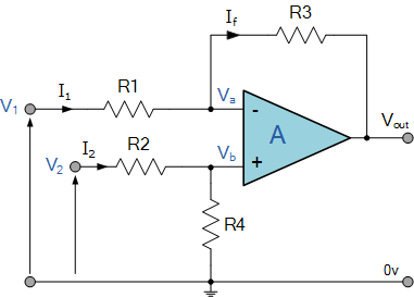
By connecting each input in turn to 0v ground, we can use superposition to solve for the output voltage Vout. The transfer function for the differential amplifier circuit is then:
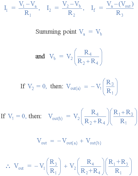
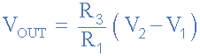
When the resistors R1 = R2 and R3 = R4, the transfer function of the above differential amplifier can be simplified to the following expression:
Differential Amplifier Formula
If all resistors have the same ohmic value, that is: R1 = R2 = R3 =
If R4 is used, the circuit will become a unity gain differential amplifier and the voltage gain of the amplifier will be exactly 1 or unity. The output expression will then simply be Vout = V2 – V1.
Also note that if input V1 is higher than input V2, the sum of the output voltages is negative, and if V2 is higher than V1, the sum of the output voltages is positive.
This differential amplifier circuit is a very useful operational amplifier circuit and by adding more resistors R1 and R2 in parallel with the input resistors
R3, the resulting circuit can either "add" or "subtract" the voltage applied to their respective inputs. One of the most common ways of doing this is to connect a "resistor bridge" (often called a Wheatstone bridge) to the inputs of the amplifier, as shown below.
Wheatstone bridge differential amplifier circuit
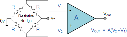
Now, a standard differential amplifier circuit works by "comparing" one input voltage to another, thus becoming a differential voltage comparator. For example, by connecting one input to a fixed reference voltage established on one branch of a resistor bridge network, and the other input to a "thermistor" or "photoresistor", the amplifier circuit can be used to detect low or high changes in temperature or light levels when the output voltage becomes a linear function of changes in the active leg of the resistor bridge, as explained below.
Light-activated differential amplifier
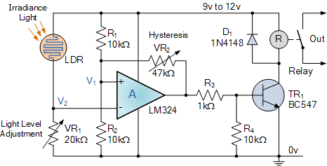
Here, the above circuit is used as a light-operated switch which turns the output relay "ON" or "OFF" when the light intensity detected by the LDR resistor exceeds or falls below a certain preset value. The fixed reference voltage is applied to the non-inverting input terminal of the operational amplifier through the R1-R2 voltage divider network.
The voltage value at V1 sets the trip point of the op amp via feedback potentiometer VR2, which is used to set the switching hysteresis. That is the difference between the light level at "ON" and the light level at "OFF".
The second leg of the differential amplifier consists of a standard light dependent resistor (also called an LDR), a light resistance sensor that changes its resistance value with the amount of light on its cell (hence the name, as its resistance value is a function of illumination).
The LDR may be any standard type of cadmium sulfide (cdS) photoconductive cell, such as the common NORP12, which has a resistance range of about 500Ω in sunlight to about 20kΩ or more in the dark.
The NORP12 photoconductive cell has a spectral response similar to that of the human eye, making it ideal for use in lighting control type applications. The photocell resistance is proportional to the light intensity and will drop as the light intensity increases, so the voltage level at V2 will also vary above or below the switch point, which is determined by the position of VR1.
Then, by adjusting the light trip or set position with potentiometer VR1, and adjusting the switch hysteresis with potentiometer VR2, a precision light-sensitive switch can be made. Depending on the application, the output of the op amp can switch the load directly, or use a transistor switch to control a relay or the light itself.
This simple circuit configuration can also be used to detect temperature by replacing the photoresistor with a thermistor. By swapping the positions of VR1 and the LDR, this circuit can be used to detect light or dark, or hot or cold with a thermistor.
A major limitation of this amplifier design is its lower input impedance compared to other op amp configurations, such as the non-inverting (single-ended input) amplifier.
Each input voltage source must drive a current through an input resistor whose total impedance is less than that of the op amp inputs alone. This may be good for low impedance sources (such as the bridge circuit above), but not so good for high impedance sources.
One way to solve this problem is to add a Unity gain buffer amplifier to each input resistor, such as the voltage follower shown in the previous tutorial. This gives us a differential amplifier circuit that has very high input impedance and low output impedance because it consists of two non-inverting buffers and a differential amplifier. This forms the basis of most "instrument amplifiers".
Instrumentation Amplifier
Instrumentation amplifiers are very high gain differential amplifiers with high input impedance and single-ended output. Instrumentation amplifiers are primarily used to amplify very small differential signals from strain gauges, thermocouples, or current sensing devices in motor control systems.
Unlike a standard op amp whose closed-loop gain is determined by an external resistive feedback connected between its output terminals and one of its input terminals, an "instrumentation amplifier" has an internal feedback resistor that is effectively isolated from its input terminals, and the op amp's positive or negative feedback is applied when an input signal is applied to its two differential inputs, V1 and V2.
The instrumentation amplifier also has a very good common-mode rejection ratio, CMRR (V1 = V
2) is well over 100dB at DC. A typical example of a three op amp instrumentation amplifier with high input impedance (Zin) is as follows:
High Input Impedance Instrumentation Amplifier
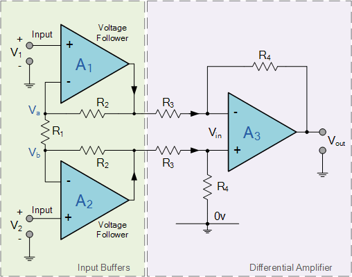
The two non-inverting amplifiers form a differential input stage and act as a buffer amplifier with a gain of 1 + 2R2/
R1, the gain of the common-mode input signal is unity. Since amplifiers A1 and A2 are closed-loop negative feedback amplifiers, we can expect the voltage at Va to be equal to the input voltage V1. Similarly, the voltage at Vb is equal to the voltage at V2.
Since the op amp has no current flowing through its input terminals (virtual ground), the same current must flow through the three resistor network of R2, R1, and R2 connected across the output of the op amp. This means, the voltage at the upper end of R1 will be equal to V1 and the voltage at the lower end of R1 will be equal to V2.
This creates a voltage drop across resistor R1 that is equal to the voltage difference between inputs V1 and V2 (the differential input voltage) because the voltage at each amplifier’s summing junction, Va and Vb, is equal to the voltage applied to its positive input.
However, if a common-mode voltage is applied to the amplifier inputs, the voltages on both sides of R1 will be equal and no current will flow through this resistor. Since no current flows through R1 (and therefore through the two R2 resistors), amplifiers A1 and A2 will operate as unity-gain followers (buffers). Since the input voltage at the outputs of amplifiers A1 and A2 appears different across the three-resistor network, the differential gain of the circuit can be varied by changing the value of R1.
The output voltage of differential op amp A3, acting as a subtractor, is simply the voltage difference between its two inputs (V2 - V1), amplified by the gain of A3, which may be 1, unity, or zero (assuming R3 =
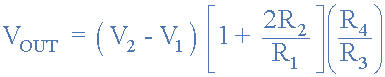
R4). We then have a general expression for the overall voltage gain of the instrumentation amplifier circuit:
Instrumentation Amplifier Formulas
- What is the difference between MOSFET and BJT? Which one is better between MOSFET and BJT?
- What is the function of a voltage regulator in a circuit? How to connect a voltage regulator?
- Analysis of the flow direction of transistor current
- What is the difference between single-phase and three-phase power? When is three-phase power required?
- What is the relationship between capacitance and impedance in an AC circuit? How do you calculate the impedance of a capacitor?
- How to identify common mode interference? Methods to eliminate common mode interference
- How to read resistor color codes? Resistor color codes illustrated
- RC filter explained in detail
- Simple Wired Spy Bug Circuit Built Based on IC741
- Share an interesting LED decoration project
- Differential amplifier emitter negative feedback gain control circuit
- High input impedance differential amplifier
- INA105 differential amplifier circuit with gain of 1
- Photodiode differential amplifier circuit
- Variable gain differential amplifier circuit
- Differential Amplifier Circuit Allowing 100V Common Mode Input Voltage
- Differential amplifier circuit with equal input impedance
- High resistance DC differential amplifier circuit
- Differential amplifier circuit with a bandwidth of 20MHZ
- 555 square wave oscillation circuit


 京公网安备 11010802033920号