What is the mechanism of microcontroller latch-up?
Source: InternetPublisher:王达业 Keywords: Single chip microcomputer latch effect Updated: 2025/02/18
What is the "latch effect"? This is a bit unfamiliar to newcomers who have just started to develop single-chip microcomputers. The single-chip microcomputer development engineer explained that from the structural point of view, the single-chip microcomputer is composed of a large number of PN junctions. There is a part composed of a quadruple structure "PNPN" in which two PN junctions are connected. The structure of PNPN is the structure of the "thyristor" used as a power switching element, and the PNPN part in the single-chip microcomputer is called a "parasitic thyristor".
According to the microcontroller development engineer, the thyristor consists of three terminals: anode (positive), cathode (negative), and gate (gate). Normally, current does not flow from the anode to the cathode, but when a signal is input to the gate, current flows from the anode to the cathode. Once the current starts to flow, it will continue to flow unless the power is turned off. Since the on-resistance at this time is very small, a large current flows. The phenomenon in which the same phenomenon occurs in the parasitic thyristor of the microcontroller is called "latch-up".
When a microcontroller latches up, a large current flows inside, causing not only non-operational failure, but also possible melting of the wires inside the microcontroller and damage to the components. Latch-up will not occur if used correctly, but if you start the power supply incorrectly or steep high-voltage noise enters the pins, latch-up will occur. Figure 1 is a picture of the metal wiring on the surface of the microcontroller that has actually been melted by the latch-up current.
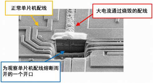
Figure 1: Latch-up current melts the metal wires on the surface of the microcontroller
1. What is the structure of a thyristor?
Figure 2 shows the structure of a thyristor (PNPN). When a positive potential is applied to the anode and a negative potential is applied to the cathode, no current flows from the anode to the cathode because J1 and J3 are forward and J2 is reverse.
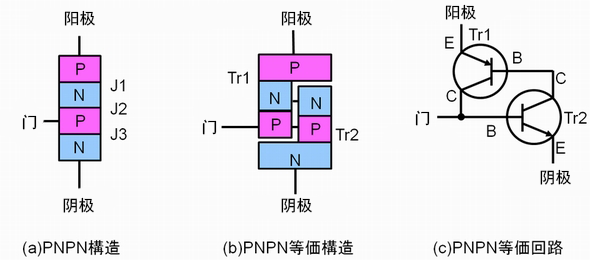
Figure 2: Thyristor structure
However, when voltage is applied to the gate and current flows, the reverse current of J2 is accelerated by the gate current, and the current flows through J2. Since J1 and J3 are forward-facing in nature, when this phenomenon occurs, current begins to flow from the anode to the cathode.
Once current begins to flow, it will continue to flow unless the anode power supply is turned off.
This is the thyristor switching operation. Using this operation, thyristors are used as switching elements in power equipment.
The PNPN junction is considered to be a combination of a PNP transistor and an NPN type as shown in Figure 2-b. The circuit diagram shows a dual transistor configuration as shown in Figure 2-c.
The emitter (E) of Tr1 becomes the anode of the thyristor, the base is the collector (C) of Tr1, the base (B) of Tr2, and the cathode is the emitter (E) of Tr2.
2. What is the mechanism of latch-up?
Figure 3 shows two transistors used in a single-chip CMOS.
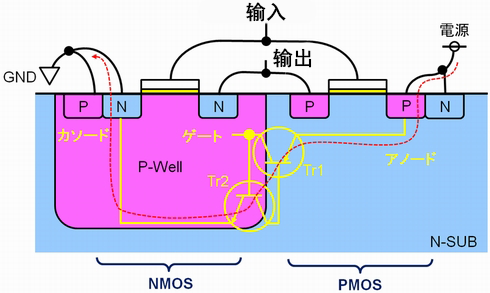
Figure 3: Latch-up mechanism
The example in the figure above is for N-SUB. In addition, there is the case of P-SUB, but in both cases a parasitic PNPN junction is formed, so the principle of latch-up can be considered in the same way.
Tr1 is formed by the Pch of the source of the PMOS, which is connected to the power supply of the N-SUB and then to the P-WELL. Then, Tr2 is formed by the Nch path from the N-SUB to the source of the NMOS of the P-WELL and GND.
Tr1 and Tr2 are formed as shown by the yellow line in the CMOS of Figure 3. The power supply side is the anode, the GND side is the cathode, and the gate is equivalent to an NMOS P-WELL.
The CMOS input line is connected to the gate of the NMOS. The gate and P-WELL form the same structure as a capacitor with the gate oxide film inserted. Capacitors easily pass high-frequency signals, so if noise enters the input line and the dV/dt of the noise is large (high-frequency component is large), it will pass through the gate oxide film and reach the P-WELL. This will trigger the PNPN junction to turn on, causing a large current to flow from the power supply to GND.
In addition, if the power line fluctuates sharply, especially if it fluctuates to the negative side, the gate voltage will be higher than the power supply voltage, and the state will be the same as when noise enters the gate. This state occurs if a voltage is applied to the terminal before the power supply of the microcontroller is established.
The MCU development engineer said that since there are countless PNPN junctions inside the MCU, we cannot know which PNPN junction will cause latch-up.
- How to display numbers on 7 segment display using 8051 microcontroller?
- How to use 8051 microcontroller to control stepper motor?
- What is the difference between RISC-V, ARM and x86 microprocessors?
- Are more bits in an MCU better?
- How to Make a PIC Programmer
- Sample and hold amplifier AD9101 interface circuit
- Digital signal isolation interface circuit
- How to use ESP8266 to design a portable air quality monitoring station
- Serial debugger circuit implemented with several discrete components
- Cable test circuit
- Design of temperature detection circuit implemented by single chip microcomputer
- Single chip multi-microcomputer system sharing RAM circuit
- PCF8591 hardware interface (circuit diagram pin diagram)
- Analysis of internal reset circuit diagram of microcontroller
- PNP and NPN transistor switching circuits
- Minimum system interface circuit based on AT89C52 microcontroller
- Signal input circuit a
- A microcontroller infrared asynchronous communication port circuit diagram
- Multi-channel DA and microcontroller optical and electrical interface circuit
- The interface between DAC1231 and microcontroller 8031


 京公网安备 11010802033920号