Advantages and Disadvantages of Negative Feedback Circuits, Analysis of Operational Amplifier Feedback Circuits
Source: InternetPublisher:拿铁三分糖 Keywords: operational amplifier negative feedback negative feedback circuit Updated: 2025/02/14
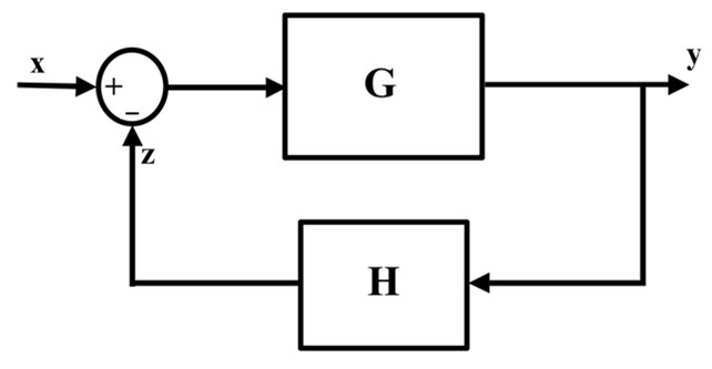
The main concerns of electronic systems are stability and accuracy, and in order to maintain these critical factors, some part of the output needs to be connected back to the input of the system, which is called feedback.
Control systems are classified into two types based on the feedback connections such as closed-loop system and open-loop system. An open-loop control system does not contain any feedback path whereas a closed-loop system contains a feedback path for automatic error correction.
Based on the nature of feedback, closed loop systems are classified into two types, they are positive feedback system and negative feedback system. In a positive feedback system, the feedback is added to the input signal.
In negative feedback signal, a certain amount of signal is subtracted from the input signal to regulate the output. The system that works based on the negative system is called "Negative Feedback Circuit". This is also called "Degenerative Feedback".
The basic block diagram of a negative feedback system is shown below, with X, Y, and Z as input, output, and feedback loop respectively.
1. Transistor feedback circuit
A disadvantage of circuits designed with transistors is that characteristics such as gain, distortion, input and output resistance, and signal-to-noise ratio depend on the characteristics of the transistor. This difficulty can be overcome by introducing negative feedback. Negative feedback reduces distortion in the circuit and enables us to control the input and output to the desired level.
1. Feedback in emitter follower circuit
The emitter follower circuit is shown in the figure below. The emitter of the transistor is grounded through a resistor, and the output is measured at the parallel node of the emitter and the grounded resistor.
BE is the voltage drop between the base and emitter of the transistor, and the negative feedback operation of the emitter follower circuit can be expressed as Vin = VBE + Vout.
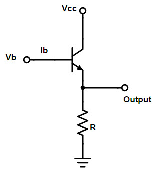
Now V BE = V in – V out. If the feedback quotient of the circuit, B = 1, then the gain can be calculated as A = 1/B = 1.
2. Advantages of emitter follower circuit
This emitter follower circuit offers two main advantages:
It provides current amplification without providing any voltage gain
It provides impedance matching.
3. Common emitter circuit feedback
The common emitter circuit is shown in the figure below. The emitter of the transistor is connected to ground through a resistor Re and the output is measured at the parallel node of the collector and the source resistor Rc.
When VBE is the voltage drop between the base and emitter of the transistor, the input to the common emitter circuit can be expressed as Vin = VBE + iERE. The output of this circuit is Vout =
-i Ç ř Ç。
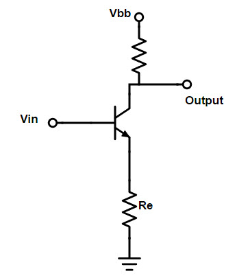
There are two methods to introduce negative feedback in a common emitter transistor. The two methods are as follows:
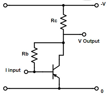
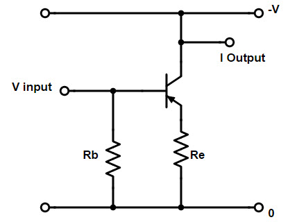
The circuits in Figures a and b above are the same circuit, using different negative feedback connection methods.
2. Operational Amplifier Feedback Circuit
The op amp circuit connected with feedback is called “op amp feedback circuit”. There are two applications of op amp with negative feedback connection. They are non-inverting op amp circuit and inverting op amp circuit.
1. Common-mode op amp circuit
The non-inverting operational amplifier circuit is shown below. The input of this circuit is connected to the non-inverting terminal of the operational amplifier and the feedback signal is connected to the inverting terminal which is connected to ground through a resistor. Therefore it has a high input impedance.
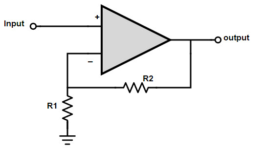
We can easily determine the gain of a non-inverting op amp. Since the voltages at both inputs are the same, the gain of the op amp will be very high. Assuming no current flows into the op amp, the currents in both resistors are the same.
Since the circuit forms a voltage divider circuit, the voltage at the inverting input is the same as the voltage at the non-inverting input, which means Vin = Vout x R1 / (R1 +
R2). The gain of the non-inverting op amp can be calculated as
Vout/Vin = AV = 1 + R2/R1
This can be clearly explained by the non-inverting amplifier circuit operation.
2. Common-mode amplifier
A non-inverting amplifier using an op amp is shown in the figure below, where the input is connected to the positive or non-inverting terminal of the op amp.
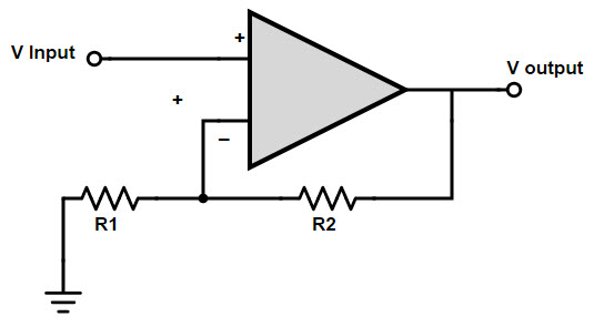
In a non-inverting amplifier, the nature of the output will be the same as the nature of the input signal. That is, if the input signal is positive, the output will also be positive, and if the input signal is negative, the output will also be negative.
3. Gain equation of operational amplifier
If the open-loop gain is AOL, the output voltage of the non-inverting op amp is:
VOut = AOL (Vin – V – ) → (1)
Where V- is a function of the output voltage, produced by the voltage divider formed by resistors R1 and R2. Since the negative terminal of the op amp will have a high impedance, this is equal to
V- = β VOut → (2)
Where β = R1 / (R1 + R2).
Now substituting equation (2) into equation (1), we obtain:
VOut = AOL (Vin – β VOut)
By solving this problem, we get:
V¬Out = Vin (1/(β+1/AOL))
If the value of AOL is high, then substituting the value of β, we get:
V¬Out = Vin (1+ R1/R2)
4. Inverting op amp circuit
The inverting op amp circuit is shown below. The input of this circuit is connected to the inverting terminal or negative terminal of the op amp and the feedback signal is also connected to the inverting terminal. The output of the inverting op amp circuit is 1800 different from its input signal.
times, and provides a virtual path.
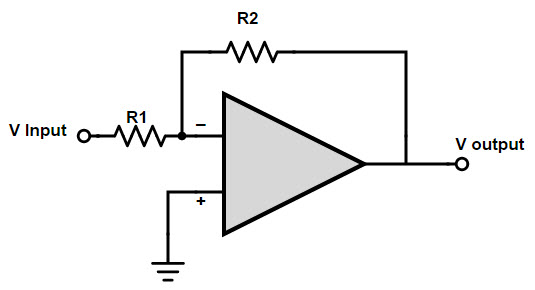
In this circuit, the input itself consumes no current. So the current flowing through resistors R1 and R2 is the same. Therefore Vout/R2 = Vin/R1. Now the circuit Av
The voltage gain is
Vout/Vin = OFF = – R2/R1
This can be clearly explained by the inverting amplifier circuit operation.
5. Inverting amplifier
An inverting amplifier using an op amp is shown in the figure below, where the input is connected to the negative or inverting terminal of the op amp.
In an inverting amplifier, the nature of the output will be opposite to the nature of the input signal. That is, if the input signal is positive, the output will also be negative, and similarly, if the input signal is positive, the output will also be negative.
6. Gain equation of operational amplifier
We can use the output voltage equation for the non-inverting op amp circuit to find the gain of the inverting op amp circuit.
VOut = AOL (Vin – V – ) → (1)
Here V – is calculated by the voltage divider formed by R f and R in, and is a function of the input and output voltages (Vout and Vin). So
V – = 1/(R f + R in ) (R f V in + R in V out ) → (2)
Now substituting equation (2) into equation (1), we obtain:
Vout = -Vin. (A(OL).Rf)/(Rf + Rin + A(OL).Rin)
If the open-loop gain value AOL is very high, then:
VOut = -Vin (1+ R f /R in )
Sometimes, a resistor is inserted between the ground and the non-inverting output of the op amp to reduce the input offset voltage due to the bias current voltage drop. This reduces the distortion of the op amp. To eliminate unwanted DC current, a DC blocking capacitor is connected in series with the input of the op amp.
3. Advantages of Negative Feedback
(1) Negative feedback can stabilize almost any type of disturbance or noise that occurs.
(2) It is used to overcome the nonlinearity of the system.
(3) It helps us flatten the frequency response of the system and allows us to obtain the desired frequency response curve. (Reduce frequency distortion)
(4) Negative feedback makes the system less dependent on the temperature and other external characteristics of the system.
(5) It increases the input resistance, i.e. it increases the input impedance
(6) Reduce output resistance, that is, reduce output impedance
(7) Increase the bandwidth of the output signal
(8) Reduce the system’s sensitivity to external characteristics.
(9) Provide bias point stability and better CMMR.
4. Disadvantages of Negative Feedback
(1) Connecting negative feedback will reduce the overall gain of the system.
(2) If the system is not designed properly, oscillation may occur.
- Why do we need a MOSFET gate resistor? MOSFET Gate Resistor Placement
- Which TVS diodes are suitable for RS232/RS485 and Controller Area Network applications?
- Principle set of zero-crossing detection circuit advantages and disadvantages
- Ideal characteristics of operational amplifiers/pin configurations/gain types/primary applications
- Classification and characteristics of operational amplifiers, classification and characteristics of operational amplifiers
- Working principle and truth table of JK flip-flop
- TL494 pin functions/configuration/ratings/operating conditions/layout diagram
- Ceramic filter structure/working principle/characteristics/application
- Tutorial on building a NOT gate using BJT transistors
- Structural diagram and function of sliding resistor
- LT108 bridge temperature measurement circuit
- Practical amplifier circuit c composed of operational amplifier LM386
- Low output impedance operational amplifier circuit
- High input impedance buffer amplifier circuit
- Output voltage expansion circuit a
- Typical circuit of three-terminal fixed stabilizer a
- Tacho generator voltage negative feedback circuit
- Operational amplifier analog switching circuit with high interference immunity
- Constant current source circuit diagram of operational amplifier and Darlington transistor
- Infrared receiving circuit using operational amplifier


 京公网安备 11010802033920号