TL494 pin functions/configuration/ratings/operating conditions/layout diagram
Source: InternetPublisher:赔钱虎 Keywords: TL494 pin function Updated: 2025/01/07
IC TL494 is designed for single chip pulse width modulation application circuits. This device is mainly used in power supply control circuits which can be dimensioned efficiently using this IC.
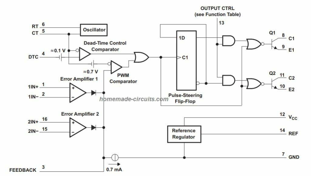
The device contains a variable oscillator, a dead-time controller stage (DTC), a trigger control for pulse steering, a precision 5 V regulator, two error amplifiers, and some output buffering circuitry.
The common-mode voltage range of the error amplifier is -0.3 V to VCC - 2V.
The dead-time control comparator is set with a fixed offset value to provide a constant dead-time of approximately 5%.
The on-chip oscillator function can be overridden by connecting the IC's RT pin #14 to the reference pin #14 and supplying a sawtooth signal externally to CT pin #5. This facility also allows synchronous driving of many TL494s with different supply rails.
IC.
The output transistors with floating outputs inside the chip are arranged to provide common emitter output or emitter follower output facilities.
The device allows the user to obtain either push-pull or single-ended oscillation on the output pins by appropriately configuring pin #13 (output control function pin).
Internal circuitry makes it impossible for any output to produce double pulses, and the IC uses push-pull functionality.
Pin Function and Configuration
The following diagram and description provide us basic information about the functionality of the pins of IC TL494.
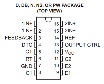
Pin #1 and Pin #2 (1 IN+ and 1 IN-): These are the non-inverting and inverting inputs of the error amplifier (op amp 1).
Pin #16, Pin #15 (1 IN+ and 1 IN-): As mentioned above, these are the non-inverting and inverting inputs of the error amplifier (op amp 2).
Pin #8 and Pin #11 (C1, C2): These are outputs 1 and 2 of the IC and they are connected to the collectors of the respective internal transistors.
Pin #5 (CT): This pin needs to be connected to an external capacitor to set the oscillator frequency.
Pin #6 (RT): This pin needs to be connected to an external resistor to set the oscillator frequency.
Pin #4 (DTC): This is the input to the internal op amp that controls the dead time operation of the IC.
Pin #9 and Pin #10 (E1 and E2): These are the outputs of the IC and are connected to the emitter pin of the internal transistor.
Pin #3 (Feedback): As the name implies, this input pin is used to integrate with the output sample signal to achieve the desired automatic control of the system.
Pin #7 (Ground): This pin is the ground pin of the IC and needs to be connected to 0 V of the power supply.
Pin #12 (VCC): This is the positive power supply pin for the IC.
Pin #13 (O/P CNTRL): This pin can be configured to enable the output of the IC in either push-pull mode or single-ended mode.
Pin #14 (REF): This output pin provides a constant 5V output and can be used to fix the reference voltage for the error op amp in comparator mode.
Absolute Maximum Ratings
(VCC) Maximum supply voltage not to exceed = 41 V
(VI) Maximum voltage on input pins does not exceed = VCC + 0.3 V
(VO) Maximum output voltage at the collector of the internal transistor = 41 V
(IO) Maximum current on internal transistor collector = 250 mA
Maximum IC lead soldering heat at 1.6 mm (1/16 inch) from IC body not to exceed 10 seconds @ 260 °C
Tstg Storage temperature range = –65/150 °C
Recommended operating conditions
The following data gives you the recommended voltages and currents that can be used to operate the IC under safe and efficient conditions:
VCC power supply: 7 V to 40 V
VI amplifier input voltage: -0.3 V to VCC - 2 V
VO transistor collector voltage = 40, collector current of each transistor = 200 mA
Feedback pin current: 0.3 mA
fOSC oscillator frequency range: 1 kHz to 300 kHz
CT Oscillator timing capacitor value: between 0.47 nF and 10000 nF
RT Oscillator Timing Resistor Value: Between 1.8 k and 500 k ohms.
Internal layout
- What is a Half Wave Rectifier? Working Principle of a Half Wave Rectifier
- RC filter explained in detail
- What is a D flip-flop and how does it work?
- Diode-based clipping circuit
- DIY a decorative lamp
- How to Build a Simple Temperature Indicator Circuit Using NTC and PTC Thermistors
- Why use PWM? What are its advantages?
- Using an Op Amp to Drive a Simple and Practical Power Amplifier
- LED Night Light
- Common electrical circuits: frequency-selective (bandpass) amplifier circuit
- AD7730 internal functional block diagram and pin function diagram
- AD7710 internal functional block diagram and pin function diagram
- IB31 internal functional block diagram and pin function diagram
- RCV420 pin function diagram
- LM311 pin function and arrangement
- Switching power supply circuit composed of TL494 integrated circuit
- Application of TL494 as current regulator
- Application of TL494 in DC motor speed control
- TL494 internal equivalent circuit diagram
- Typical application circuit diagram of TL494


 京公网安备 11010802033920号