SiC MOSFET isolated gate driver with PCB based transformer
Source: InternetPublisher:明天见 Keywords: Gate Driver SiC MOSFET Updated: 2025/08/19
This article describes a transformer-based isolated gate driver for 3.3kV SiC MOSFETs. Two VHF-modulated resonant flyback converters operating at 20 MHz generate the PWM signals and gate drive power.
High-voltage isolation (15 kV RMS) is provided by a PCB-based air-core transformer. This transformer features a low coupling capacitance of 5 pF, enhancing noise immunity even under the high dv/dt of the SiC MOSFET. To evaluate the effectiveness of the proposed solution, experimental results using a 3.3 kV discrete SiC MOSFET are presented.
Isolated gate drivers
The typical configuration of an isolated gate driver (GD) for a high-voltage SiC MOSFET is shown in Figure 1 (a). An isolated gate drive power supply (GDPS) is required, and optical fiber (OF) is often used to transmit the gate PWM signal to ensure sufficient isolation and low parasitic capacitance on the signal path [1], [5]. The disadvantages of this solution are the high cost of optical fiber and the need for at least two isolated power supplies.
An alternative solution has been proposed based on a 20kV isolated GDPS with a transformer based on PCB windings [2]. Although it has low coupling capacitance (<2pF), it results in a bulky transformer due to the gap distance between the core and the PCB windings.
Wireless power transfer (WPT) converters [3], [5] and GDPS based on optical power transfer [3], [4] allow you to eliminate the coupling capacitance but achieve low transmission power (< 1W) and conversion efficiency (< 25%). Inductive power transfer GDPS uses a single-turn primary winding to power multiple secondary receivers [5], where the low coupling capacitance is achieved by a wide air gap between the primary winding and the magnetic core. However, if the primary transmitter fails, all secondary-side gate voltages will be out of control.
The novel solution proposed in this paper is shown in Figure 1(b). By using a PCB-based air-core transformer with high dielectric strength, an RMS insulation voltage of 15 kV is achieved. Furthermore, the low coupling capacitance enhances the 3.3 kV SiC MOSFET's high dv/dt noise immunity.
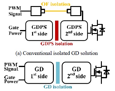
Figure 1: Traditional and proposed isolated GD solutions
Schematic diagram
Figure 2 shows a schematic diagram of the proposed solution. On the primary side, the PWM signal is modulated with a VHF signal (20 MHz) to generate gate signals for two RFCs. The first RFC is active when the PWM signal is high (1), while the second is active when the PWM signal is low (0). Regardless of the PWM duty cycle, the output voltage VO of both stages maintains a constant DC value. Therefore, the power received by the secondary side is independent of the PWM duty cycle.
On the secondary side, two envelope detectors connected to the anodes of diodes DR1 and DR2 detect the on/off state of the RFC. These edge-detected signals are then buffered as PWM rising and falling edges and sent to the RS bi-stable, which regenerates the PWM signal. A non-isolated DC-DC regulator connected after RFC 1 provides the required +5V, +15V, and -5V drive voltages for the secondary-side signal processing circuitry.
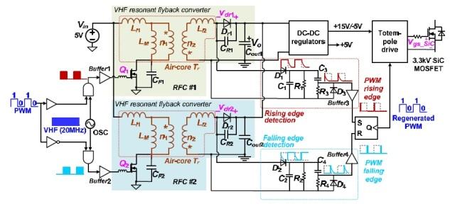
Figure 2: Schematic diagram of the proposed GD solution
The relevant waveforms are shown in Figure 3.
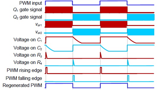
Figure 3: Key waveforms of the proposed GD
transformer
The PCB-based air-core transformer design, shown in Figure 4, offers the advantage of eliminating core losses and potential insulation issues between the windings and the core. It utilizes a stacked PCB structure, comprising a primary PCB, a transformer (Tr)-PCB, and a secondary PCB. The transformer windings have a spiral shape to simplify the design. The Tr-PCB has only two layers, with the primary and secondary windings located on the top and bottom layers, respectively. With this solution, insulation is entirely provided by the Tr-PCB's dielectric material (typically low-cost FR-4).
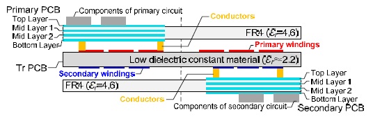
Figure 4: Structure of a PCB-based transformer
To increase the dielectric breakdown voltage and reduce the coupling capacitance, materials with high dielectric strength and low dielectric constant can be used. The authors used Arlon-DiClad-880 material, which has a dielectric constant of 2.2 and a dielectric strength greater than 45 kV/mm. The simulated coupling capacitance determined using the Ansys Q3D extractor tool was approximately 5 pF for several transformers.
The creepage distance between the coated primary and secondary windings is greater than 30 mm × 2. This ensures an insulation voltage of 15 kV RMS according to IEC-61800-5-1-2007.
Experimental results
Figure 5 shows a schematic diagram of the prototype used for testing, which was built in the laboratory using the components listed in Table I.
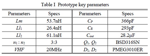
Table 1: List of components used in the prototype
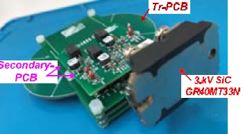
Figure 5: Prototype diagram
The RFC's maximum output power was measured at 1.5W@17Ω resistive load, sufficient to drive a 3.3kV SiC MOSFET (GR40MT33N). A graph of efficiency and RFC output voltage (VO) is shown in Figure 6. Both RFCs maintain stable output characteristics across the entire load range (0.12W-1.5W).
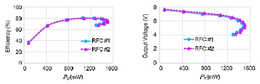
Figure 6: Efficiency and RFC output voltage
In addition, a double pulse test (DPT) is implemented to evaluate the performance of the proposed GD. The schematic diagram of the DPT test bench is shown in Figure 7.
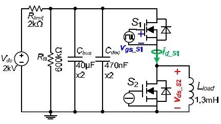
Figure 7: Schematic diagram of the DPT test bench
The GD drives switch S1, requiring high isolation voltage and noise immunity to high dv/dt. Figure 8 shows the DPT waveforms for Vdc = 2kV, id_S1,max = 44A, Lload = 1.3mH, and Rgon/Rgoff = 2.2Ω/5Ω. It can be seen that the maximum dv/dt achieved by the 3.3kV SiC MOSFET corresponds to a safe value of 100V/ns. The same GD solution can also be used for other high-voltage SiC MOSFET devices.
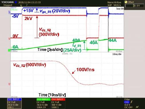
Figure 8: Experimental waveform
- Electronic fuse
- 1.5V to 5V converter
- Power LED driver circuit
- Solar charger for USB devices
- Lithium polymer battery charging solution using MCP73833
- Fluorescent lamp inverter
- Battery reverse polarity protection circuit
- Solar-powered mobile phone charger
- Should I choose voltage mode or current mode for fixed frequency pulse width modulation (PWM) control?
- Five Easy Steps to Powering Your SoC with a PMIC
- Some brief summaries on power MOSFET applications, you deserve them
- Industrial product promotion and shopping guide DC power supply circuit
- 2-phase CPU power circuit using HIP6301 and HIP6601 chips
- KGDS type single-phase low temperature iron plated power supply circuit
- 300A-18V three-phase thyristor voltage regulating electrolytic power supply circuit
- Low voltage adjustable reference power circuit
- Practical neon light power circuit
- Common power circuits and applications 04
- DC-DC conversion power supply circuit
- JFET-MOSFET headphone circuit diagram


 京公网安备 11010802033920号