Circuit Features and Benefits
The circuit shown in Figure 1 is a fully isolated 12-bit, 300 kSPS RTD temperature measurement system using only three active devices. The system handles Pt100 RTD output and integrates innovative circuitry for lead compensation via a standard three-wire connection. This circuit operates from a single 3.3 V supply. After room temperature calibration, the total error does not exceed ±0.24% FSR over a temperature variation of ±10°C, making it ideal for a variety of industrial temperature measurement applications.
The circuit's small size makes this combination an industry-leading temperature measurement solution for temperature measurement applications where accuracy, cost and size are critical. Data and power are isolated from each other, so the circuit has excellent high voltage tolerance while also effectively avoiding ground loop interference common in harsh industrial environments.
This innovative circuit for realizing three-wire RTD lead compensation was developed by Dr. Hristo Ivanov Gigov, associate professor at the Department of Electrical Engineering and Microelectronics at Varna Technical University in Bulgaria, and engineer and doctoral student Stanimir Krasimirov Stankov.


Circuit Description
The input stage of this circuit is an RTD signal conditioning circuit, using a compensated three-wire connection to the RTD. This circuit converts the RTD input resistance range (100 Ω to 212.05 Ω, 0°C to 300°C temperature range) to a voltage level compatible with the ADC input range (0 V to 2.5 V).
The RTD excitation current is provided by op amp U1C, one quarter of the quad AD8608. The 100 mV reference voltage VR is generated by the R8/R9 divider driven by the 2.5 V ADC reference voltage, which generates VR/(R1||R2) RTD excitation current of approximately 1.05 mA.
When the temperature range is 0°C to 300°C, the excitation current produces a voltage change of approximately 117.6 mV (105 mV to 222.6 mV) across the RTD. The U1A op amp amplifies this voltage change by a factor of 19.6, producing a 2.3 V output range. Resistor R2, in parallel with resistor R1, level shifts the output range so that the U1A op amp outputs 0.1 V to 2.4 V, matching the ADC's input range (0 V to 2.5 V) while providing 100 mV headroom to maintain linearity. performance. The resistor values can be modified to accommodate other common temperature ranges described later in this circuit note.
The circuit design supports single power supply. The AD8608 has a minimum output voltage rating of 50 mV (2.7 V supply) and 290 mV (5 V supply), a load current of 10 mA, and a temperature range of −40°C to +125°C. With a 3.3 V supply, load current less than 1 mA, and a narrower temperature range, a conservative estimate of the minimum output voltage is 45 mV to 60 mV.
Taking into account device tolerances, the minimum output voltage (lower end of range) is set to 100 mV to provide a safety margin. The upper limit of the output range is set to 2.4 V to provide 100 mV of headroom for positive swings at the ADC input. Therefore, the nominal output voltage range of the op amp is 0.1 V to 2.4 V.
Op amp U1B buffers the internal 2.5 V reference voltage of the AD7091R (U3) ADC.
The AD8608 quad operational amplifier was chosen for this application because of its low offset voltage (75 μV maximum), low bias current (1 pA maximum), and low noise (12 nV/√Hz maximum) characteristics. At a 3.3 V supply, power consumption is only 18.5 mW.
The U1D operational amplifier provides a three-wire correction signal to compensate for errors caused by lead resistors r1 and r2. The gain from point A to TP1 is +19.6 and the gain from point B to TP1 is −39.2. The voltage at point A contains a positive error term equal to the voltage drop across r1 and r2. The voltage at point B contains a positive error term, the value is equal to the voltage drop on r2, and the small voltage drop on r3 can be ignored. Since the gain from point B to TP1 is negative and twice the gain from point A to TP1, the errors caused by the voltage drops across r1 and r2 cancel (assuming r1 = r2).
The output stage of the op amp is followed by a single-pole RC filter (R11/C9) to reduce out-of-band noise. The cutoff frequency of the RC filter is set to 664 kHz. In the presence of low-frequency industrial noise, an additional second-order filter (adding capacitors C10 and C11) is used to reduce the filter cutoff frequency. At this time, the AD7091R will not operate at the maximum throughput rate. To improve conversion speed, do not fill C10 and C11.
The AD7091R 12-bit 1 MSPS SAR ADC was chosen because of its ultra-low power consumption of only 349 µA at 3.3 V (1.2 mW), which is significantly lower than any competing ADC currently on the market. The input bandwidth is 7.5 MHz, and the high-speed serial interface is SPI-compatible. The AD7091R also has a built-in 2.5 V reference with a typical drift of ±4.5 ppm/oC. The AD7091R is available in a small 10-pin MSOP package.
When powered from a 3.3V supply, the total power dissipation of this circuit (not including the ADuM5401 isolator) is approximately 20 mW.
Galvanic isolation is provided by the ADuM5401 quad-channel digital isolator (Grade C). In addition to isolating the output data, the ADuM5401 provides an isolated +3.3 V power supply to this circuit. The ADuM5401 is not required for normal operation of the circuit unless isolation is required. The ADuM5401 quad-channel 2.5 kV isolator integrates a DC/DC converter and is available in a small 16-pin SOIC package. The ADuM5401 consumes approximately 140 mW at a 7 MHz clock frequency.
The AD7091R requires a 50 MHz serial clock (SCLK) to achieve a 1 MSPS sampling rate. However, the ADuM5401 (Grade C) isolator has a maximum data rate of 25 Mbps, which corresponds to a maximum serial clock frequency of 12.5 MHz. In addition, the SPI port requires that the trailing edge of SCLK drives the output data to the processor, so the total two-way propagation delay of the ADuM5401 (120 ns maximum) limits the upper clock limit to 1/120 ns = 8.3 MHz.
Although the AD7091R is a 12-bit ADC, the serial data is also formatted as 16-bit words to be compatible with the processor serial port requirements. Therefore, the sampling period TS consists of the 650 ns conversion time of the AD7091R plus 58 ns (additional time required by the data sheet, t1 delay + tQUIET delay), plus 16 clock cycles for the SPI interface data transfer.
TS = 650 ns + 58 ns + 16 × 120 ns = 2628 ns
fS = 1/TS = 1/2628 ns = 380 kSPS
To provide a safety margin, it is recommended to set the maximum SCLK and sample rate to 7 MHz and 300 respectively kSPS. The digital SPI interface can be connected to the microprocessor evaluation board using a 12-pin Pmod-compatible connector (DigilentPmod specification).


Circuit Design
The circuit shown in Figure 2 can convert an RTD resistance change of 100Ω to 212.05Ω into an output voltage change of 0.1 V to 2.4 V, compatible with the ADC input range. Additionally, this circuit eliminates
errors related to wire resistance r1 and r2.
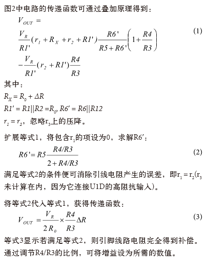
Calculation of Gain, Output Offset, Resistor Value and Tolerance
If the temperature range is 0°C to 300oC, the RTD Pt100 resistance range is 100Ω to 212.05Ω, and the input resistance change ΔR of the circuit in Figure 2 is 0Ω to 112.05Ω. Therefore, the circuit gain from Equation 3 is:


If this condition is met, then R1′ = R0 = 100 Ω at 0°C and VOUT = 0 V.
Now, the output offset of the circuit must be set to 0.1 V. A simple way to offset the output is to make resistor R1' slightly lower than R0. Note that this affects the gain proportionally. The 0.1 V output offset is approximately 4.35% of the total 2.3 V range, so the ratio R1′/R0 must be less than 0.9565. To maintain a high output level of 2.4 V, the ratio R4/R3 can be proportionally corrected. For example, R4 = 0.9565 × 41.06 × R3 =39.27 kΩ. Using the standard resistor values in Figure 1, the circuit provides a good approximation of the required gain and output offset. R1′ is formed by connecting resistor R2 = 1.91 kΩ in parallel with resistor R1 = 100 Ω.
For any other temperature range, or for any other temperature sensor (e.g. Pt200, Pt500, Pt1000, Pt2000), the resistor value must be recalculated as follows:
Select the R3 value (e.g. 1 kΩ) and then make R5 = R6 = 2R3.
Select the excitation current IR through the sensor and calculate VR = IR × RX_low where RX_low = RTD resistance at the lowest temperature in the range.
Choose a value for R9 (e.g. R9 = 1 kΩ), then calculate R8:

where VREF = 2.5 V = ADC reference voltage.
Calculate A = 0.0435 × (RX_high – RX_low) where, A = temporary constant required to complete the calculation process. RX_high = RTD resistance at highest temperature in range.
Calculate R0 = RX_low – A.
Calculate R0 = R1 × R2/(R1 + R2) and choose the R1 and R2 values. It is recommended to choose the standard R1 value so that it is equal to RX_low and then calculate R2.
Calculation

Among them, B= is the temporary constant required to complete the calculation process.
Calculate R4 = B × R3, ensuring R12 = R4.
Accuracy Analysis
Equation 1 indicates that all resistors contribute to the total error. If these values are chosen carefully, the total error caused by using alternative standard value resistors can be reduced to less than a few percent. However, the output of the U1A op amp at 100Ω and 212.05Ω inputs should be recalculated using Equation 1 to ensure that the required margin is maintained. In a real circuit, choose the resistor value that is closest to an existing standard. Resistors Rl, R2, R8, and R9 are 0.1%, 25 ppm/°C. The other resistors in the circuit are 1%, 100 ppm/°C: R3, R4, R5, R6, and R12.
The absolute accuracy of such circuits depends primarily on the resistors, so gain and offset calibration is required to eliminate errors caused by substitution of standard value resistors and resistor tolerances.
Effect of Resistor Temperature Coefficient on Total Error
Equation 1 shows that the output voltage is related to the following nine resistors: R1, R2, R3, R4, R5, R6, R8, R9, and R12.
The full-scale output voltage at TP1 is sensitive to small changes in the resistance of each of these nine resistors, and its sensitivity is calculated through a simulation program. The input RTD resistance of the circuit is 212Ω. The calculated sensitivities are SR1 = 1.83, SR2 = 0.09, SR3 = 0.94, SR4 = 0.94, SR5 = 1.35, SR6 = 1.28, SR8 = 0.97, SR9 = 0.96, and SR12 = 0.07. Assuming that the temperature coefficients are combined in a root sum square (rss) fashion, the total full-scale drift of the 25 ppm/°C resistors R1, R2, R8, and R9 and the 100 ppm/°C resistors R3, R4, R5, R6, and R12 is approximately is:
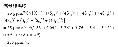
A full-scale drift of 236 ppm/°C corresponds to 0.024% FSR/°C. If the temperature changes by ±10°C, the error is ±0.24% FSR.
Using 25 ppm/°C resistors for all nine resistors reduces the full-scale drift to approximately 80 ppm/°C (or 0.008% FSR/°C).
After completing the calibration process, errors due to resistor tolerances, offsets produced by the AD8608 op amp (75 μV), and the AD7091R ADC are eliminated. It is still necessary to calculate and verify that the op amp output is within the required range.
Effect of Active Component Temperature Coefficient on Total Error
The DC offset of the AD8608 op amp (75 μV) and AD7091R ADC is removed by the calibration procedure.
The offset drift of the AD7091R ADC's built-in reference is 4.5 ppm/°C typical and 25 ppm/°C maximum.
The offset drift of the AD8608 op amp is 1µV/°C typical and 4.5µV/°C maximum.
Note that if 50 ppm/°C or 100 ppm/°C resistors are used, the largest source of total drift is resistor drift, and drift from active components is negligible.
Pin Line Resistance Compensation
The circuit in Figure 1 fully compensates for the pin line resistance (r1, r2, and r3). However, if there is any mismatch in Equation 3, pin traces r1 and r2 will introduce errors into the measurement. The third pin line r3 has no effect on the circuit because it is connected to the high impedance input of U1D.
The linearity of the circuit is not affected by pin traces r1 and r2, even if there is a mismatch in Equation 3.
RTD Linearization
The circuit in Figure 1 is linear with respect to the change in resistance of the RTD. However, the RTD transfer function (resistance versus temperature) is nonlinear. Therefore, linearization is required to eliminate the nonlinear errors of the RTD. For systems involving microcontrollers, linearization is usually accomplished in software. The AN-709 application note discusses partial linearization techniques for Pt100 RTD sensors. The same technique is used in the CN0337 evaluation software to eliminate the nonlinear errors of the Pt100 sensor.
Test data before and after two-point calibration.
In order to perform two-point calibration, a precision resistor of 100 Ω is first applied to the input end, and the ADC output code is recorded as Code_1. Then, apply a 212.05 Ω precision resistor to the input terminal, and record the ADC output code as Code_2. The gain factor is calculated by:

The error before calibration is obtained by comparing the ideal transfer function calculated using the nominal values of the components with the uncalibrated actual circuit transfer function. The test circuit is constructed using ±1%, ±100 ppm/°C resistors (except R1, R2, R8, and R9, which are ±0.1%, ±25 ppm/°C resistors). Testing was done using a printed circuit board (PCB) at room ambient temperature.
Figure 3 shows the test results before and after calibration of some test boards without changing the temperature. As shown in the figure, the maximum error before calibration is approximately 0.27% FSR. After calibration, the error is reduced to ±0.037% FSR, which is roughly equivalent to the ADC's 1.5 LSB error.


PCB layout considerations
In any circuit where precision is important, power and ground return layout on the circuit board must be carefully considered. The PCB should isolate the digital and analog parts as much as possible. The PCB of this system is made of a simple double-layer board stack, but better EMS performance can be obtained by using a 4-layer board. See the MT-031 guide for a detailed discussion of layout and grounding, and the MT-101 guide for information on decoupling techniques. The AD8608 power supply should be decoupled with 10µF and 0.1µF capacitors for proper noise suppression and ripple reduction. These capacitors should be as close to the corresponding devices as possible, and the 0.1µF capacitors should have low ESR values. For all high frequency decoupling, ceramic capacitors are recommended. Power traces must be as wide as possible to provide a low impedance path and reduce the effects of glitches on the power lines. The ADuM5401 isoPower integrated DC/DC converter requires power supply bypassing on the input and output power pins. Note that low ESR bypass capacitors are required between Pins 1 and 2 and between Pins 15 and 16, and these should be placed as close to the chip pads as possible. To suppress noise and reduce ripple, at least two capacitors need to be connected in parallel. For VDD1 and VISO, the recommended capacitor values are 0.1µF and 10µF. Smaller capacitors must have low ESR, ceramic capacitors are recommended. The total trace length from the end of the low ESR capacitor to the input power pin must not exceed 2 mm. If the bypass capacitor trace length exceeds 2 mm, data may be corrupted. Consider bypassing between Pin 1 and Pin 8 and Pin 9 and Pin 16 unless the two common ground pins are tied together close to the package. Please refer to the ADuM5401 data sheet for more information.
For a complete documentation package, including schematics, board layout and bill of materials (BOM), please refer to: www.analog.com/CN0337-DesignSupport.
High Voltage Capability
This PCB is designed according to the 2500 V basic insulation specification. High voltage testing above 2500 V is not recommended. Caution must be exercised when using this evaluation board at high voltages, and this PCB must not be relied upon for safety functions as it has not been high potential tested (also known as high voltage testing or withstand voltage insulation testing) and has not been safety certified.


 京公网安备 11010802033920号

 CDLL937


