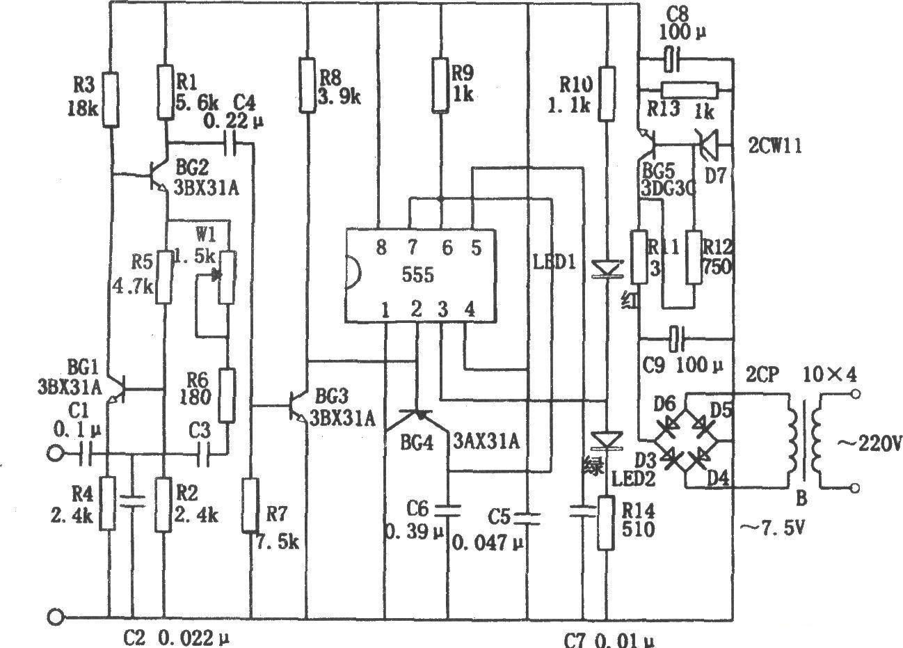
The circuit shown in Figure 1 is a 16-bit, 250 MSPS, narrowband, high-IF receiver front end that provides the optimal interface between the ADL5565 differential amplifier and the AD9467 ADC.
The AD9467 is a buffered input 16-bit, 200 MSPS or 250 MSPS ADC with SNR performance of approximately 75.5 dBFS and SFDR performance between 95 dBFS and 98 dBFS. Due to its high input bandwidth, low distortion, and high output linearity, the ADL5565 differential amplifier is suitable for driving intermediate frequency sampling ADCs.
This circuit note presents a systematic process for designing interface circuits and anti-aliasing filters to ensure minimum signal loss while maintaining high performance. Use the resonant matching method to design the flattest Butterworth fourth-order bandpass filter with a center frequency of 200 MHz.


The advantages of using a differential amplifier to drive a high-speed ADC include signal gain, isolation, and ADC to source impedance matching. The ADL5565 allows pin-strapped gain adjustment of 6 dB, 12 dB, or 15.5 dB. Alternatively, finer gain steps can be achieved from 0 dB to 15.5 dB by applying two external resistors to the input. In addition, the ADL5565 features high output linearity, low distortion, low noise, and wide input bandwidth. 3 dB bandwidth is 6 GHz and 0.1 dB flatness is 1 GHz. The ADL5565 can achieve an output third-order intercept point (OIP3) greater than 50 dB.
To achieve the optimal level of performance that the ADL5565 and AD9467 have to offer, the design principles specified in each data sheet must be strictly followed. Some of the design guidelines include properly matching the input and output impedances of the ADL5565 for minimum signal loss and optimal linearity, using systematic design of anti-aliasing filters to improve dynamic range, and source impedance matching the ADC input, etc.
ADL5565 input impedance matching


Figure 2 shows the input matching network recommended for use with the ADL5565. The input impedance of the ADL5565 is gain-dependent, with a differential input impedance of 200 Ω at 6 dB gain, 100 Ω at 12 dB gain, and 67 Ω at 15.5 dB gain. To match the 50 Ω source impedance of the signal generator to the input impedance of the ADL5565, R1 and R2 must be selected so that their sum equals 50 Ω in parallel with the ADL5565 input impedance ZI. To maintain balance within the differential circuit, R1 must equal R2. The following formula can be used to calculate the necessary matching resistors.

Table 1 shows the calculated termination resistors and pin configurations for different gain settings of the ADL5565.
An alternative to the configuration shown in Figure 2 is to replace the 1:1 balun ETC1-1-13 with an impedance conversion RF transformer. This eliminates the need for R1 and R2. A 1:4 transformer can be used for the 6 dB gain configuration, and a 1:2 transformer can be used for the 12 dB gain configuration. The advantages of this alternative configuration are lower component count and lower signal loss. However, attention should be paid to the bandwidth of the transformer. Compared to a 1:1 balun, an impedance conversion transformer has a narrower bandwidth and higher insertion loss.

Figure 2 shows the single-ended to differential method of driving the ADL5565 using a balun or transformer. This configuration may not be feasible or necessary in some applications. The driver interface of the ADL5565 is flexible and can be driven single-ended (shown) or differentially using a differential mixer. Please refer to the ADL5565 data sheet for details on the different input interfaces.
ADL5565 output load matching
The ADL5565 linearity performance is optimized for a 200 Ω output load. This is a common output impedance used in interfacing with ADCs and in filter designs. With an optimized output load of 200 Ω, the ADL5565 has an output IP3 of 46 dBm at 200 MHz.
If a 200 Ω output load is not suitable for the application, there is a trade-off between the ADL5565's output load and linearity performance. Figure 3 shows a plot of third-order intermodulation (IMD3) versus common output load frequencies.


AD9467 source impedance
The AD9467 is an ideal ADC choice in this circuit because it is an intermediate-frequency sampling ADC optimized for high performance over a wide bandwidth and ease of use. The AD9467 has an integrated buffer to provide a fixed input impedance to the driver amplifier. This input structure is superior to ADCs that use an unbuffered front end coupled directly to the sampling switch. An unbuffered ADC provides a time-varying input sample-and-hold impedance to the driver amplifier. Adding an input buffer relaxes the driver requirements, but at the cost of slightly higher power consumption. The buffered source impedance of the AD9467 is modeled as a fixed impedance of 530 Ω in parallel with a 3.5 pF capacitor.
When interfacing with an ADC, it is recommended to subtract the true input impedance from 530 Ω to a lower value in the range of 200 Ω to 400 Ω. By lowering the input impedance of the ADC, kickback caused by the sample-and-hold structure settles faster, thereby improving linearity performance. The downside is the increase in input power since driving the full-scale ADC requires more power. In this circuit example, the input impedance of the AD9467 is reduced to 200 Ω to match the output impedance of the ADL5565 and balance linearity with ADC input power dissipation. The input impedance of the AD9467 is reduced to 200 Ω by placing a 310 Ω resistor in parallel with the ADC differential input.
Anti-aliasing filter design
The anti-aliasing filter in front of the ADC helps reduce signal components and noise in the unwanted Nyquist zone, thereby avoiding in-band aliasing and degrading dynamic performance. Anti-aliasing filters are usually designed using LC networks. In order to obtain the required stopband and passband characteristics, the source impedance and load impedance must be selected appropriately. For example, filter design can be accomplished using software provided by Nuhertz Technologies or Agilent Technologies' Advanced Design System (ADS).
In the circuit shown in Figure 1, an ADS program is used to design a fourth-order flattest (Butterworth) low-pass filter. Figure 4 shows a low-pass filter design with source and load impedances of 200 Ω and a 3 dB cutoff frequency of 300 MHz. The 200 Ω impedance was chosen because it is a common source and load impedance for driver amplifiers and ADCs. The first components are series inductors used to relax driver requirements.
In the final optimized circuit in Figure 1, the filter source impedance is approximately equal to 21.6 Ω; however, for the low-pass part of the filter design, 200 Ω was chosen because the overall filter is ultimately a resonant bandpass filter, and more importantly , the amplifier and ADC must accept the correct load and source impedance to achieve optimized linearity performance. The result is amplitude loss due to impedance mismatch.


The low-pass filter design is further tuned by establishing resonance to produce peaking within the target frequency band. In this way, a narrow-band, band-pass filter at high and medium frequencies is obtained. Placing an inductor across the ADC's differential input zeros out the ADC's input capacitance and establishes peaking. Figure 5 shows the calculation used to determine the resonant inductance value. In the case of the AD9467's 3.5 pF source impedance, a parallel inductance of 181 nH is required to zero the capacitive susceptance; the result is only the high-impedance resistive portion of the RC parallel equivalent resistance. The resonant frequency chosen for the calculation is 200 MHz.


Measuring performance
Figure 1 shows the final circuit configuration. Each output of the ADL5565 is padded with 5.6 Ω to improve driver amplifier stability. The recommended series resistance generally ranges from a few ohms to tens of ohms. Larger resistor values improve stability; but the downside is power loss because the series resistor together with the impedance at the ADC input creates a voltage divider, causing signal attenuation.
Following the series resistor at the ADL5565 output is a 1 nF DC blocking capacitor. This is followed by an anti-aliasing filter, followed by a 310 Ω parallel resistor to reduce the input impedance of the ADC. Finally, a 15 Ω resistor is placed in series with the ADC input to isolate internal switching transients from the filter and amplifier.
Figures 6 and 7 show the resulting anti-aliasing filter responses, with a 1 dB bandwidth of 41 MHz and a 3 dB bandwidth of 89 MHz, centered at the 203 MHz IF. Figure 8 shows the FFT spectrum of the final receiver circuit shown in Figure 1, where the SNR is 72.5 dBFS and the SFDR performance is close to 90 dBc.


The filter elements can be further tuned using ADS as a simulation tool to shift the resonant peak to the desired intermediate frequency. For example, changing the antialiasing filter's parallel 8.2 pF capacitance to 10 pF reduces the resonant spike to 180 MHz. Figures 9 through 11 show the filter curves and single-frequency FFT performance under this condition.


Blockdiagram
All reference designs on this site are sourced from major semiconductor manufacturers or collected online for learning and research. The copyright belongs to the semiconductor manufacturer or the original author. If you believe that the reference design of this site infringes upon your relevant rights and interests, please send us a rights notice. As a neutral platform service provider, we will take measures to delete the relevant content in accordance with relevant laws after receiving the relevant notice from the rights holder. Please send relevant notifications to email: bbs_service@eeworld.com.cn.
It is your responsibility to test the circuit yourself and determine its suitability for you. EEWorld will not be liable for direct, indirect, special, incidental, consequential or punitive damages arising from any cause or anything connected to any reference design used.
Supported by EEWorld Datasheet
EEWorld
subscription
account

EEWorld
service
account

Automotive
development
community

Robot
development
community

About Us Customer Service Contact Information Datasheet Sitemap LatestNews


Room 1530, 15th Floor, Building B,
No.18 Zhongguancun Street,
Haidian District,
Beijing, Postal Code: 100190
China
Telephone: 008610 8235 0740
 京公网安备 11010802033920号

 177-710-1-15GP4J7-24RDN