The quadrature demodulator provides an in-phase (I) signal and a quadrature (Q) signal that is exactly 90° out of phase. The I and Q signals are vectors, so the amplitude and phase shift of the received signal can be calculated using trigonometric identities, as shown in Figure 2. The local oscillator (LO) input is the original transmit signal, and the RF input is the receive signal. The demodulator generates a sum and difference term. The RF and LO signals have exactly the same frequency, ω LO = ω RF , so the result is that the high frequency sum term is filtered out and the difference term resides at DC. The phase of the received signal (φ RF ) is different from the phase of the transmitted signal (φ LO ), and this phase shift can be expressed as φ LO −φ RF .


Real I/Q demodulators have many flaws, including quadrature phase errors, gain imbalance, LO-RF leakage, etc., all of which result in degraded demodulated signal quality. To select a demodulator, first determine the RF input frequency range, amplitude accuracy, and phase accuracy requirements. The ADL5380 demodulator operates from a single 5 V supply and accepts RF or IF input frequencies from 400 MHz to 6 GHz, making it ideal for receiver signal chains. Depending on the configuration, providing 5.36 dB of voltage conversion gain, the ADL5380's differential I and Q outputs can drive a 2.5 V pp differential signal into a 500 Ω load. At 900 MHz, it has a noise figure (NF) of 10.9 dB, a first-order intercept point (IP1) of 11.6 dBm, and a third-order intercept point (IP3) of 29.7 dBm, with excellent dynamic range; and 0.07 dB Amplitude balance and 0.2° phase balance achieve outstanding demodulation accuracy. The ADL5380 is fabricated using an advanced SiGe bipolar process and is available in a small 4 mm × 4 mm, 24-pin LFCSP package.
ADC Drivers and High-Resolution Precision ADCs The
ADA4940-2 fully differential dual-channel amplifier features excellent dynamic performance and adjustable output common-mode voltage, making it ideal for driving high-resolution dual-channel SAR ADCs. The ADA4940-2 operates from a single 5 V supply and provides a ±5 V differential output with a 2.5 V common-mode voltage. Depending on the configuration, it provides a gain of 2x (6 dB) and drives the ADC input to full scale. An RC filter (22 Ω/2.7 nF) limits noise and reduces kickback from the capacitive digital-to-analog converter (DAC) at the ADC input. The ADA4940-2 is manufactured using a patented SiGe complementary bipolar process and is available in a small 4 mm × 4 mm, 24-pin LFCSP package.
The AD7903 dual-channel, 16-bit, 1 MSPS SAR ADC provides excellent accuracy with an FS gain error of ±0.006% and an offset error of ±0.015 mV. The AD7903 operates from a single 2.5 V supply and consumes only 12 mW at 1 MSPS. The main goal of using a high-resolution ADC is to achieve ±1° phase accuracy, especially when the DC amplitude of the input signal is small. The 5 V reference required by the ADC is generated by the ADR435 low noise reference.


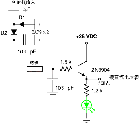
Blockdiagram
All reference designs on this site are sourced from major semiconductor manufacturers or collected online for learning and research. The copyright belongs to the semiconductor manufacturer or the original author. If you believe that the reference design of this site infringes upon your relevant rights and interests, please send us a rights notice. As a neutral platform service provider, we will take measures to delete the relevant content in accordance with relevant laws after receiving the relevant notice from the rights holder. Please send relevant notifications to email: bbs_service@eeworld.com.cn.
It is your responsibility to test the circuit yourself and determine its suitability for you. EEWorld will not be liable for direct, indirect, special, incidental, consequential or punitive damages arising from any cause or anything connected to any reference design used.
Supported by EEWorld Datasheet
EEWorld
subscription
account

EEWorld
service
account

Automotive
development
community

Robot
development
community

About Us Customer Service Contact Information Datasheet Sitemap LatestNews


Room 1530, 15th Floor, Building B,
No.18 Zhongguancun Street,
Haidian District,
Beijing, Postal Code: 100190
China
Telephone: 008610 8235 0740
 京公网安备 11010802033920号

 MCH182AN103KK