The ADV7612 is a dual-port Xpressview™ 225 MHz HDMI® receiver with fast switching between two inputs. Figure 1 shows a circuit using two ADV7612s as a four-input fast-switching HDMI receiver.
This circuit demonstrates the scalability of the ADV7612 in applications requiring four multiplexed HDMI inputs up to 225 MHz TMDS (1080p60, 12 bits per channel; 148.5 MHz LLC pixel clock) or UXGA (1600 × 1200, per Channel 10 bit; 162 MHz LLC pixel clock). It is an economical solution for this application and operates over the extended industrial temperature range of −40°C to +85°C.


The ADV7612 provides a receiving solution for dual HDMI inputs. Figure 1 shows how to connect two ADV7612s in parallel on a shared video and audio bus to multiplex four HDMI inputs. It also shows how to set up I2C communication and switch between signal sources without causing bus conflicts. A software package is also provided showing how to handle communication and authentication in an HDMI repeater application (see http://ez.analog.com/community/video ).
The device must be controlled from the I2C bus in a non-conflicting manner. The board layout of this circuit is critical and should follow straight-line principles and use controlled impedance to reduce the risk of reflections and cross-coupling. The complete PCB layout is included in the design support package, which can be downloaded from: www.analog.com/CN0224-DesignSupport . The ADV7511 HDMI transmitter is used as the back-end device.
Bus output status
After reset, the ADV7612 tri-states pins P0-P35, HS, VS/FIELD/ALSB, DE, LLC, AP0…AP5, SCLK/INT2, and MCLK/INT2. These pins can be set to the active state through the registers TRI_PIX, TRI_SYNCS, TRI_LLC, TRI_AUDIO, as described in the UG-216 Hardware User Guide, please visit http://ez.analog.com/docs/DOC-1751
Video and audio bus loading
Only one ADV7612 can access the AV bus at a time; the second device must remain tri-stated. Assuming the output driver impedance (P0…P35) is 10 Ω to 20 Ω (highest drive strength) and the trace characteristic impedance is 75 Ω, a series resistor of 55 Ω to 65 Ω is required to match the characteristic impedance of the trace. The tri-state output bus driver on the ADV7612 has a maximum capacitance of 20 pF (refer to the electrical specifications in the ADV7612 data sheet ).
Layout and Termination Considerations
For this design, you must ensure that the transmission lines are properly terminated and have controlled impedance. Otherwise, reflections (which can occur on longer lines) can adversely affect the data being sent.
For pixel lines (P0…P35), video sync (VS/FIELD/ALSB, HS, DE) and audio lines (AP0, AP1/I2S_TDM, AP2…AP5, MCLK/INT2, SCLK/INT2) – except LLC , it is recommended to use a 51 Ω series termination resistor on the ADV7612 driver side, and a trace with a characteristic impedance of 75 Ω.
The Line Locked Clock (LLC) lines have the same 75 Ω characteristic impedance and should have no series resistance, but the far end should be symmetrically terminated (150 Ω to +3.3 V and 150 Ω to GND) as shown in Figure 2. Although the theoretical optimal termination value is between 50 Ω and 60 Ω, testing found that a symmetrical 75 Ω (2 × 150 Ω) termination increases the swing so that the signal is centered around the mid-supply (1.65 V). One point is ideal. The ADV7511 HDMI transmitter is included on the board and is used to send the multiplexed outputs of two ADV7612s.


Figures 3 through 6 show the waveforms for various terminations. In each case, the symmetrical LLC termination is placed at the far end (near the ADV7511) and the series termination resistor is placed as close as possible to the two ADV7612 devices, as shown in Figure 2.
Measurements were performed on the ADV7511 pins using a Tektronix P6243 FET probe (1 MΩ impedance, 1 GHz bandwidth, capacitance less than 1 pF) and a Tektronix TDS5104B oscilloscope.
As can be seen from the waveform, using a 2 × 150 Ω termination on the LLC line ensures a maximum swing of 3.3 V.
Using 75 Ω on the data lines will result in too low edge speeds. 33 Ω and 15 Ω on the data lines cause falling edge undershoot (Figure 5 and Figure 6) and rising edge overshoot (not shown). Therefore LLC chose 2 × 150 Ω and used 51 Ω on the data lines, as illustrated by the eye diagrams in Figures 9 and 10.


I 2 C access
After power-up, both ADV7612 devices will have the same I 2 C address on the master map , which may cause a conflict.
A CS CS pin is available on both devices , allowing selection of one of the two devices. After the CS line is pulled low, I 2 C communication is enabled.
When the CS line is pulled high, I 2 C communication is disabled.
A simple inverter reduces the resources required on the microcontroller side, as shown in Figure 7.


CEC
Whether CEC is implemented on a circuit board is up to the end user and is not mandatory. If CEC is not required, the CEC pin should be left floating (as described in UG-216 , Appendix B: Recommended Configuration for Unused Pins). This user guide can be downloaded from http://ez.analog.com/docs/DOC-1751 .
Alternatively, a standalone engine should be used to handle CEC commands.
XTAL_N, XTAL_P
There are two ways to drive the ADV7612 clock. The two devices can have separate crystal oscillators connected to the XTAL_N and XTAL_P pins, or they can share the same signal clock. In this circuit, the 1.8 V signal clock from the oscillator is provided to the pin XTAL_P of the two devices. In this configuration, XTAL_N must remain floating. Proper wiring and grounding layout must be ensured to eliminate coupling between sensitive lines. Each trace of the bus should be the same length.
interrupt
Interrupts from both devices must be considered. The ADV7612 has two possible interrupts: INT1 (INT1 pin) and INT2 (provided via SCLK/INT2, MCLK/INT2 or HPA_A/INT2).
It is not recommended to use INT2 via pins MCLK/INT2 or SCLK/INT2, tri-stating the audio bus via the TRI_AUDIO register will also tri-state these pins.


Layout considerations
The layout should consist of very short traces. Ideally, the trace connecting two pins of the same function between two ADV7612s should be as short as possible and should share the same series termination resistor, which is placed as close as possible to both devices and then connected to the bus. In practice, this requirement is impossible to meet due to layout constraints; therefore each device requires its own series termination resistor (see Figure 2). Video traces should be as close to the same length as possible to provide delay matching.
Assessment and testing
This circuit was evaluated using two video generators (Quantum Data 882) to generate UXGA 1600 × 1200 pixel, 30-bit and 1080p60, 36-bit video (Samsung2 and MoirèX patterns). Use Astro VA-1831 video analyzer as HDMI receiver (output from ADV7511). Additionally, connect the P6243 (1 pF, 1 MΩ, 1 GHz) probe to the Tektronix TDS5104B oscilloscope and observe the ADV7612 video signal (LLC and P35) on the ADV7511 pin. The resulting waveforms are represented as eye diagrams using the ADV7511 eye mask. Figures 9 and 10 show UXGA video of the Samsung2 pattern (162 MHz, 30 bits). The MoirèX pattern used during testing also showed similar safety margins.

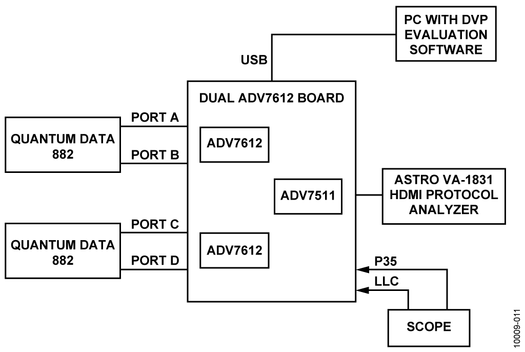
Measuring video timing via Astro VA-1831 shows no anomalies. Analysis of MoirèX's even and odd vertical lines (1080p60 36-bit and UXGA 30-bit) shows that all bits are switched correctly at the same time without any leakage between lines (MoirèX pattern). The Astro VA-183 also showed stable HDMI sync signals and packets with correct CRC checksums. This shows that the backend ADV7511 correctly receives the clock and synchronization information.
Test steps


Blockdiagram
All reference designs on this site are sourced from major semiconductor manufacturers or collected online for learning and research. The copyright belongs to the semiconductor manufacturer or the original author. If you believe that the reference design of this site infringes upon your relevant rights and interests, please send us a rights notice. As a neutral platform service provider, we will take measures to delete the relevant content in accordance with relevant laws after receiving the relevant notice from the rights holder. Please send relevant notifications to email: bbs_service@eeworld.com.cn.
It is your responsibility to test the circuit yourself and determine its suitability for you. EEWorld will not be liable for direct, indirect, special, incidental, consequential or punitive damages arising from any cause or anything connected to any reference design used.
Supported by EEWorld Datasheet
EEWorld
subscription
account

EEWorld
service
account

Automotive
development
community

Robot
development
community

About Us Customer Service Contact Information Datasheet Sitemap LatestNews


Room 1530, 15th Floor, Building B,
No.18 Zhongguancun Street,
Haidian District,
Beijing, Postal Code: 100190
China
Telephone: 008610 8235 0740
 京公网安备 11010802033920号

 C0402C123C1PA


