This circuit utilizes the AD5542 voltage output DAC , the ADR421BRZ voltage reference , and the AD8628 auto-zero op amp used as a reference buffer to achieve precision data conversion. The AD8628 reference voltage buffer provides feature advantages previously only available in expensive auto-zero or chopper-stabilized amplifiers. These zero-drift amplifiers use Analog Devices' circuit topology to combine low cost with high accuracy and low noise. No external capacitors are required, and the digital switching noise associated with most chopper-stabilized amplifiers is greatly reduced, making this amplifier an excellent choice for reference buffering.
This circuit can achieve precision, low power consumption, voltage output digital-to-analog conversion. AD5542 has two operating modes: buffered mode and non-buffered mode. Which operating mode is best depends on the specific application and its settling time, input impedance, noise, etc. requirements. The output buffer amplifier can be selected based on DC accuracy or fast settling time requirements. If the DAC is required to drive loads below 60 kΩ, output buffering is required. The output impedance of the DAC is constant and independent of the digital code, but to minimize gain error, the input impedance of the output amplifier should be as high as possible. The output amplifier should also have a 3 dB bandwidth of 1 MHz or higher. The output amplifier adds another time constant to the system, thus extending the settling time of the final output.
The higher the amplifier's 3 dB bandwidth, the faster the effective settling time of the DAC and amplifier combination. All components in the circuit can operate from a single +5 V supply. The input voltage range of the ADR421 reference is 4.5 V to 18 V.

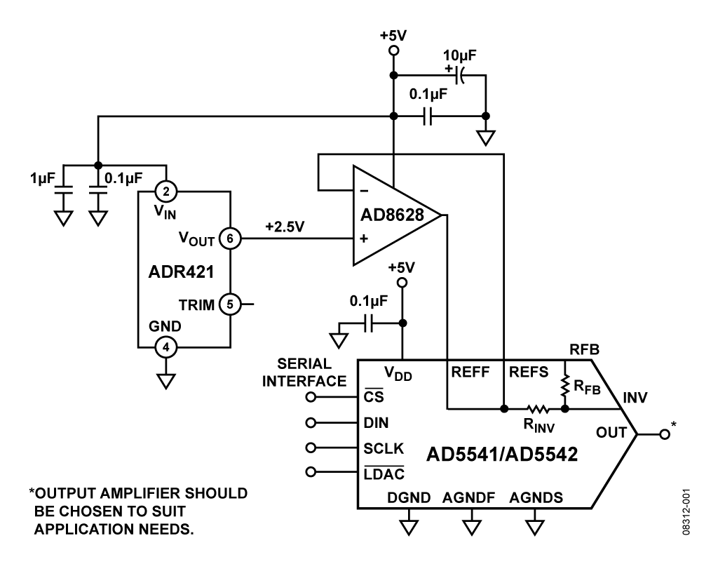
This circuit uses the AD5542 voltage output DAC, which provides 16-bit, high-precision performance. The DAC architecture of the AD5541 /AD5542 is a segmented R-2R voltage mode DAC. With this configuration, the output impedance is independent of the digital code, while the input impedance of the reference is highly dependent on the digital code. Therefore, the selection of the reference voltage buffer is very important for the handling of code-dependent reference current. If the DAC reference voltage buffer is insufficient, linearity errors may result. When selecting a reference buffer for use with a precision voltage output DAC, the op amp's offset voltage, offset error temperature coefficient, and noise are important selection criteria. Offset errors in the reference circuit can cause gain errors at the DAC output. This circuit uses the AD8628, a zero-drift, single-supply, rail-to-rail input/output op amp, which has an offset voltage of 1 μV, a drift of less than 0.005 μV/°C, and a noise of 0.5 μV peak-to-peak (0.1 Hz to 10 Hz), making it suitable Applications where error sources need to be minimized. The output voltage is related to the reference voltage as shown in the following equation:
![]()
Where D is the decimal digital word loaded into the DAC register, and N is the resolution of the DAC.
For a 2.5 V reference voltage, the above equation simplifies to the following:
![]()
Therefore, the V OUT corresponding to the mid-scale code is 1.25 V, and the V OUT corresponding to the full-scale code is 2.5 V.
The LSB size is 2.5 V/65,536 = 38.1 μV.
There is a common misconception that autozero amplifiers are unreliable because internal switching actions can cause intermodulation terms and allow unwanted harmonics to enter the output unfiltered. Previous auto-zero amplifiers used auto-zero or chopper stabilization technology. Traditional auto-zero technology makes the noise energy at the auto-zero frequency lower, but due to the aliasing of broadband noise in the auto-zero frequency band, it will cause low-frequency Noise is higher. Chopping technology results in lower low-frequency noise, but the noise energy at chopping frequencies is larger. The AD8628 series adopts a patented ping-pong configuration and uses both auto-zero and chopper technology to achieve lower low-frequency noise and lower energy at chopping and auto-zero frequencies, thereby reducing signal-to-noise in most applications. The ratio is the highest and no additional filtering is required. The internal chopping frequency is relatively high (15 kHz), thus simplifying the requirements for efficient, noise-free, wide-bandwidth filters in instrumentation and process control applications.
The measurement results show that using the AD8628 as a reference voltage buffer in a high-precision, high-performance system can achieve high accuracy, low noise, and lowest high-frequency intermodulation distortion (referred to the output) performance.
Integral nonlinearity (INL) error refers to the deviation of the actual DAC transfer function from the ideal transfer function, expressed in LSB. Differential nonlinearity (DNL) error is the difference between the actual step size and the ideal value of 1 LSB. The circuit shown in Figure 1 has an INL error of ±1 LSB and a DNL error of ±1 LSB at 16-bit resolution. Figures 2 and 3 show the INL and DNL performance of this circuit.


The measured offset error and gain error are 10 μV and 170 μV respectively. The gain error of ±5 LSB and the zero-code error of ±1 LSB are within the specified error range of 38 μV (2.5 V reference, ambient temperature).
Figure 4 shows the 0.1 Hz to 10 Hz noise plot for this circuit. The output VOUT of the DAC is connected to the input of a 0.1 Hz to 10 Hz bandwidth filter followed by an amplifier with a gain of 10,000. Using an oscilloscope to capture the voltage noise, a very low peak-to-peak voltage of 57 mV (relative to the DAC output of 5.7 μV) was observed.


Figure 5 shows the DAC output obtained using a spectrum analyzer, swept from 100 Hz to 100 kHz. No significant intermodulation distortion (IMD) term was observed, indicating that an auto-zero amplifier such as the AD8628 is an excellent choice as a reference voltage buffer.


In any circuit where precision is important, careful consideration of the power supply and ground return layout on the circuit board helps achieve the goal. The printed circuit board (PCB) containing the circuit should have separate analog and digital sections. If this circuit contains other devices in the system that require an AGND to DGND connection, the connection can only be made at one point. This ground point should be as close as possible to the AD5542. The power supply to the AD5542 should be bypassed with 10 μF and 0.1 μF capacitors. These capacitors should be as close to the device as possible, preferably directly opposite the device with the 0.1 μF capacitor. The 10 μF capacitor is a tantalum bead type capacitor. The 0.1 μF capacitor must have low effective series resistance (ESR) and low effective series inductance (ESL), which are typically found in common ceramic capacitors. The 0.1 μF capacitor provides a low-impedance path to ground for high frequencies caused by transient currents caused by internal logic switches. Power traces should be as wide as possible to provide a low impedance path and reduce the effects of surges on the power lines. Clocks and other fast-switching digital signals should be shielded by digital ground so that they are not affected by other components on the board.
This circuit must be built on a multilayer circuit board with a large area ground plane. For optimal performance, proper layout, grounding, and decoupling techniques must be used (refer to Tutorial MT-031, “Grounding Data Converters and Unraveling the Mystery of AGND and DGND” , and Tutorial MT-101, — "Decoupling Technology" ).


Blockdiagram
All reference designs on this site are sourced from major semiconductor manufacturers or collected online for learning and research. The copyright belongs to the semiconductor manufacturer or the original author. If you believe that the reference design of this site infringes upon your relevant rights and interests, please send us a rights notice. As a neutral platform service provider, we will take measures to delete the relevant content in accordance with relevant laws after receiving the relevant notice from the rights holder. Please send relevant notifications to email: bbs_service@eeworld.com.cn.
It is your responsibility to test the circuit yourself and determine its suitability for you. EEWorld will not be liable for direct, indirect, special, incidental, consequential or punitive damages arising from any cause or anything connected to any reference design used.
Supported by EEWorld Datasheet
EEWorld
subscription
account

EEWorld
service
account

Automotive
development
community

Robot
development
community

About Us Customer Service Contact Information Datasheet Sitemap LatestNews


Room 1530, 15th Floor, Building B,
No.18 Zhongguancun Street,
Haidian District,
Beijing, Postal Code: 100190
China
Telephone: 008610 8235 0740
 京公网安备 11010802033920号

 100-4P6-T1-B12-M71-R-E-HDW15


