Smart WIFI socket based on Tuya WR2 module
Introduction
Sockets are a common and indispensable application tool in people's daily lives. However, most people forget to unplug the electrical equipment when they are not in use. This phenomenon is very common, which causes a waste of electrical energy and poses safety risks. . This article introduces a WIFI smart socket based on Tuya module, which can realize remote device power-off and scheduled power-on and off functions. Smart sockets provide a convenient and safe electricity environment for people's lives.
Keywords smart socket Tuya WR2 module timing
Tuya Smart is a global cloud development platform, AI+IOT developer platform, connecting the intelligent needs of consumers, manufacturing brands, OEM manufacturers and chain retailers. Products can be quickly made intelligent through the Tuya IOT platform. Developers reduce the amount of development tasks on the product side and the cloud. I would like to thank Tuya and Lichuang for co-organizing this event, allowing more civilian enthusiasts to get in touch with IOT and develop the products they want.
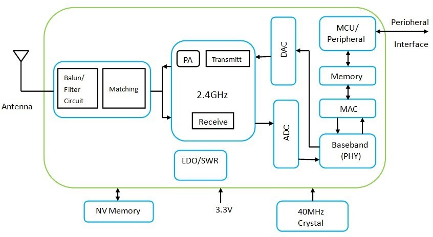
This smart WIFI socket uses Tuya WR2 module. WR2 is a low-power embedded Wi-Fi module developed by Hangzhou Tuya Information Technology Co., Ltd. It consists of a highly integrated wireless radio frequency chip RTL8710BN and an external flash chip. It has built-in Wi-Fi network protocol stack and rich library functions. WR2 also includes low-power ARM CM4F, WLAN MAC, 1T1R WLAN, with a maximum frequency of 125MHz, built-in 256K SRAM, 2Mbyte flash and rich peripheral resources. WR2 is an RTOS platform that integrates all Wi-Fi MAC and TCP/IP protocol function libraries. Users can develop embedded Wi-Fi products that meet their own needs based on these.
The structure diagram of WR2 is shown in Figure 1.1:
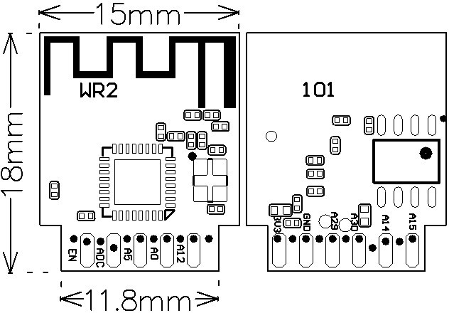
Size package
WR2 has a total of 2 rows of pins (2×9), and the pin spacing is 1.5mm.
WR2 size: 15 mm (W) × 18 mm (L) × 3.3 mm (H), the package is shown in Figure 2.1:
Figure 2.1 WR2 Dimensional Drawing
Pin definition
General pin definitions are shown in Table 2.1:
Table 2.1 WR2 pin arrangement description
| pin | symbol | IO type | Function |
|---|---|---|---|
| 1 | VD33 | P | Module power pin (3.3V) |
| 2 | GPIOA_12 | I/O | GPIOA_12 |
| 3 | GND | P | Power reference ground |
| 4 | GPIOA_0 | I/O | GPIOA_0, it cannot be pulled high at the moment of power-on. It can be configured after power-on. |
| 5 | GPIOA_29 | I/O | UART_Log_RXD (used to print module internal information) |
| 6 | GPIOA_5 | I/O | GPIOA_5 |
| 7 | GPIOA_30 | I/O | UART_Log_TXD (used to print module internal information) |
| 8 | ADC | AI | ADC port, maximum input voltage 5V |
| 9 | GPIOA_14 | I/O | GPIOA_14 |
| 10 | CHIP_EN | I/O | External enable reset pin (active low level) |
| 11 | GPIOA_15 | I/O | GPIOA_15 |
Note: P represents the power pin, I/O represents the input and output pin, and AI represents the analog input pin.
The above information can be found in Tuya module information. We only need to know the definition of each pin and the working voltage. For specific circuit connections, please refer to the module reference circuit.
According to the project function, we need a power circuit, load control circuit (relay), buttons, indicator lights, and graffiti modules. The final circuit schematic diagram drawn is as follows:
 2.1 Main components
SY50252FAC: Non-isolated LED driver chip, used here to provide 5V power supply for the circuit and power supply for the relay.
AMS1117-3.3: Linear regulated power supply, which steps down 5V to 3.3V to power the module.
WR2 WiFi module: responsible for connecting to WiFi and issuing instructions through the APP to control the relay action.


When soldering the circuit, in addition to ensuring that there are no false soldering, false soldering, or empty soldering, the welding sequence is first low and then high, with resistance and capacitance first and then IC.
The welding process is omitted.
After welding the power supply part, conduct a power test first. The success or failure depends entirely on the power supply. As a result, something went wrong. The power chip exploded when I turned on the power. I checked the schematic and found the problem. I was really careless and lost more than 4 yuan...
The board can only jump wires now. Everyone in the group is worried about jumpers. I am secretly happy that mine can't jump wires. All right. . Before jumping the wires, change the schematic diagram first. You can compare it with the above schematic diagram to see the problem. .

After the PCB jumper is powered on, the 5V output and 3.3V output voltages are normal. Look at the devastated board
 The voltage is normal, let's start welding the module.
Pictures after welding the module

A power supply casing is installed. The WIFI indicator light uses the original light guide pillar of the power supply casing. I mark a hole for the button and use a glue stick to make a button. It can also guide light and can be pressed, killing two birds with one stone.
 Tuya APP is very simple to operate. It is easy to get started, and the network configuration is also simple and easy to configure by following the steps.


After this activity, I think I have really made a product. I have been using it at home for 3 days now. I have set morning and evening schedules on the Tuya APP to control the electric blanket at home, so that it is warm when I get into bed! ! Hahaha
1. This time the schematic diagram and PCB drawing mainly consist of two issues:
1) I didn’t read the specifications of the power chip thoroughly and made a mistake in drawing the basic circuit, which resulted in burning two chips.
2) When drawing the PCB, only a single relay was selected. An additional commonly used package should be placed on it to facilitate the use of high-power loads later.
2. Regret
The original project set for this event was "Smart Water Heating Electric Blanket Based on Tuya Module". I wanted to use the MCU+ module mode to completely embed the circuit into the existing finished product at home. It can set the temperature, timing, and temperature sampling. , water shortage alarm, over-temperature alarm and other functions. Because of my work, I have less spare time and I don’t have enough time to implement it. Let’s make up for this regret little by little later.
Anyway, thanks to Tuya and Lichuang.

All reference designs on this site are sourced from major semiconductor manufacturers or collected online for learning and research. The copyright belongs to the semiconductor manufacturer or the original author. If you believe that the reference design of this site infringes upon your relevant rights and interests, please send us a rights notice. As a neutral platform service provider, we will take measures to delete the relevant content in accordance with relevant laws after receiving the relevant notice from the rights holder. Please send relevant notifications to email: bbs_service@eeworld.com.cn.
It is your responsibility to test the circuit yourself and determine its suitability for you. EEWorld will not be liable for direct, indirect, special, incidental, consequential or punitive damages arising from any cause or anything connected to any reference design used.
Supported by EEWorld Datasheet
EEWorld
subscription
account

EEWorld
service
account

Automotive
development
community

Robot
development
community

About Us Customer Service Contact Information Datasheet Sitemap LatestNews


Room 1530, 15th Floor, Building B,
No.18 Zhongguancun Street,
Haidian District,
Beijing, Postal Code: 100190
China
Telephone: 008610 8235 0740
 京公网安备 11010802033920号

 T520X107M003ASE015


