Table of contents
This project was originally planned to be completed during the summer vacation, but because I went to the company for an internship, it was postponed for a while. Today I am going to start from scratch and complete the project seriously. I will record the completion time of each stage of my project as well as my thoughts and analysis on the topic. Everyone can make progress together. Today is August 29, 2020, and I officially started designing this project. Face it calmly, think carefully and find ways, let's work hard together! !
Let me tell you again why I chose this topic? Personally, I am good at hardware, because I made a drone (motor driven) when I was in fifth grade, but I gave up this hobby due to the pressure of study. I originally wanted to do wireless charging of smart cars, but I felt that Dynamic aspects require software cooperation. It is a bit difficult to do it by yourself, so I chose the 2013 question A which is purely about hardware. In fact, there is also a power supply question that is okay, such as the question A in 2015 about bidirectional DC_DC converter, and the question K in 2017 about single-phase power analysis. Detector, as well as the 2019 Question C line load and fault detector.
Lei Chaolin, Mark Lei
Born in 2000 in Hengyang, Hunan.
Electronic and electrical major, focusing on integrated circuit testing technology and high-frequency signal processing
Award-winning experience (chronological order)
Published the paper "Research on stm32 and PID Algorithm" in April 2020
First Prize in the Electronic Design Competition of the Ministry of Science, Technology and Innovation in July 2020
Outstanding students of Lichuang Internet of Things summer practical training camp in August 2020
First Prize in the Academy’s Embedded Design Competition in September 2020
Provincial first prize in Hunan Province Electronic Design Competition (TI Cup) in October 2020
The first person recommended for the electrical major in the 2021 Hunan Provincial Vocational College Skills Competition Provincial First Prize (Integrated Circuit Application and Development)
To be continued…
 The picture above shows the work report to the director of Hunan Provincial Department of Science and Technology (first from left)
 topic:
By analyzing the basic requirements of the question, boosting and filtering are what we often use. I think the difficulty is relatively average, but it is not easy to do well. I have just started to use XL6019 for boosting. This BOOST boosting chip supports 10V-32V input, outputs about 34-38V, and has a switching frequency of about 50Khz. The voltage can be adjusted according to the FB pin. This chip is in my in the requirements list.
After reading several other question requirements, I found that PFC technology is somewhat difficult, and others are relatively easy. In terms of power supply for the entire system (not boost, but microcontroller power supply), I chose to use the buck-type BUCK chip LM2596. This chip There are countless applications. When considering whether to use ADJ or a fixed voltage output model, considering the power loss of the chip, I used the LM2596 12V fixed voltage output, which not only supports wide voltage input (10-35V) but also has 98% efficiency.
LM2596 internally contains a 150KHZ oscillator, 1.23v reference voltage stabilizing circuit, thermal shutdown circuit, current limit circuit, amplifier, comparator and internal voltage stabilizing circuit. Because the input voltage is more than 30V, if the 7812 linear voltage regulator chip is used, a large amount of heat will be generated, causing the chip to not work properly.
The picture above shows the typical application circuit of XL6019
Chip heat dissipation problem: LM2596 has two packaging forms, 5-pin TO-220(T); TO-263(S). Generally, the TO-220(T) package requires a heat sink.
The size of the heat sink is determined by input voltage, output voltage, load current and ambient temperature. The higher the ambient temperature, the higher the demand for heat dissipation.
The LM2596 in the TO-263(S) package is a surface mount component that needs to be soldered on the PCB board. Copper and the PCB board help dissipate the heat of this packaged device, such as the freewheeling diode and inductor.
The copper area on the PCB for soldering this packaged device should be at least 0.4 square inches. More copper area will improve the thermal characteristics, but above 6 square inches, the improvement in heat dissipation will be very small.
It should be used under ventilated conditions, so I plan to make this high-power circuit a separate PCB. This will not only facilitate testing, but also increase heat dissipation efficiency.
The picture above shows the LM2596 package with better heat dissipation effect.
Then let’s analyze what PFC technology is:
With the emphasis and application of power factor correction (PFC) technology in our country, research on dedicated controllers for power factor correction is gradually increasing. Considering the rapid development of CAD technology today, traditional circuit design methods have undergone revolutionary changes. Computer simulation participates in product design, which is not only efficient, safe, and cost-saving, but can also optimize system performance by adjusting parameters. In the early stages of product development, computer simulation can ignore parasitic effects, avoid noise interference, and simplify complex circuits. However, there is still little research on computer simulation models of power factor correction special controllers in China. In order to better use computer simulation to design high-frequency power conversion systems, research on computer simulation models of power factor correction special integrated circuits has been carried out. necessary.
At present, there are many varieties of PFC application-specific integrated circuits. Some foreign semiconductor manufacturers such as Motorola, Unitrode, Silicon General, Siemens, and MicroLinear have developed and produced PFC application-specific integrated circuits. Common ones include UCC28019ADR, MC34261, TDA4814, TDA4815, TDA4816, TDA4817, UC3854, ML4819, etc., dedicated to boost conversion power factor correction. The technical indicators and performance of various products are different, but their structures and functional modules are basically the same.
After checking the information, UCC28019 is an excellent factor power correction chip. With the development of electronic circuits, it has been widely used. The design of many high power factor rectifiers relies on this chip, which shows its classicity. This chip uses average current mode to correct the power factor and is suitable for wide-range universal AC input and output power factor converters from 100W to 2kW. . The chip has a fixed switching frequency (65kHz) and has many system protection functions such as peak current limit, soft overcurrent protection, open-loop detection, input power-down protection, and output overvoltage/undervoltage protection.
The functions of each pin are:
GND pin - ground;
ICOMP pin - current loop compensation, the output end of the transconductance current amplifier;
ISENSE pin - inductor current detection;
VINS pin - AC input voltage detection;
VCOMP pin - voltage loop compensation, the output end of the transconductance voltage error amplifier;
VSENSE pin - output voltage detection;
VCC pin - power input terminal;
GATE pin——gate drive output terminal
因为XL6019不支持PFC功率校正所以我放弃了XL6019 ,我将采用UCC28019ADR来进行功率矫正,同时要增加电流和电压实时采样电路,因为题目还有一项要求是电流超过2.5A时进行过载保护,根据欧姆定律,I=U/R,我们输出电压为36V,输出电流为2A,那么我们的负载电阻为18R,那么再算一下过载情况下的电阻值,为36/2.5=14.4R,这样计算之后,我们就准备一个大功率电阻,阻值可以在14R到18R之间变化,或者我们可以进行并联来调节阻值,这里我们需要注意的是必须使用大功率电阻,因为电流要达到2A,根据功率计算公式P=I的平方乘以R,我们至少要准备80W的大功率电阻,这里我们可以选择电子线性假负载,这样不仅仅方便,还可以节约成本。
在单片机控制方面,我将使用STC(国产之光)的89c52RC系列单片机,此单片机特点:
STC89C52RC是STC公司生产的一种低功耗、高性能CMOS8位微控制器,具有8K字节系统可编程Flash存储器。
拥有灵巧的8 位CPU 和在系统可编程Flash,使得STC89C52为众多嵌入式控制应用系统提供高灵活、超有效的解决方案
全静态工作,工作范围:0Hz~24MHz;
三级程序存储器加密;
1、128×8位内部RAM
2、32位双向输入输出线
3、两个十六位定时器/计数器
4、五个中断源,两级中断优先级
5、一个全双工的异步串行口
6、间歇和掉电两种工作方式
7、超强抗干扰: 高抗静电(ESD保护) ,轻松过 2KV/4KV快速脉冲干扰
8、宽电压,不怕电源抖动
9、宽温度范围,-40℃~85℃
10、禁止ALE输出
11 、掉电模式:典型功耗<0.1 μ A
12 、空闲模式:典型功耗2mA
13 、正常工作模式:典型功耗4mA-7mA
14 、掉电模式可由外部中断唤醒,适用于电池供电系统,如水表、气表、便携设备等
单片机选择好之后,我们就要开始来构建系统框架,这样不仅仅方便我们去设计,还方便程序的调试,不会突然忘记
以上为程序框架
这个单片机模块我打算单独做一块电路板,与采样电路集成到一起,刚开始我是想把采样电路与升压电路放一起
但是由于后期调试中发现升压路的高频信号对采样的精度有影响,这让我想起我学长拿不锈钢盆罩着精密运放模块!
吹口气电压就会飘!哈哈
于是我将采样与升压电路板分开,防止电路受升压模块干扰。
有了这些充足的准备,实现题目要求就非常容易了。接下来我就要开始画电路图了。
上图为第一个版本,后续还要继续修改
1、主电源电路
2、辅助电源
3、主采样电路
4、过载保护
5、单片机电路
6、显示模块
7、辅助采样电路
1.4.1 主升压模块
UCC28019ADR
前面已经介绍了UCC28019这款可以矫正PFC的电源功率芯片,现在让我们来看看怎么去设计外围电路
UCC28019具体有以下保护功能
(1)软启动(SS)
(2)VCC脚欠压锁定(UVLO)
(3)输入掉电保护(IBOP)
(4)输出过压保护(OVP)/输出欠压保护(UVD)
(5)开环保护/待机模式(OLP/Standby)
(6)过流保护
(4)栅极驱动
开关器件的参数选取
开关器件的最大峰值电流IDS_PEAK(max)可通过以下公式计算
Uin为我们输入电压34V,Uout为我们输出电压36V,Pout为输出最大功率。
我通过计算得知我需要5A以上的MOS管,这里我选择了IRF540,
D2为了是更快关闭mos管,R12为保护电阻,防止击穿开关芯片
输入滤波电容的选取
在允许有20%的电感电流纹波IRIPPLE和6%的高频电压纹波UIN_RIPPLE的情况下,输入滤波电容的最大值CIN由输入电流纹波IRIPPLE和输入电压纹波UIN_RIPPLE(max)决定。输入滤波电容的值可通过以下公式计算:
通过计算,我选择了470uF*2的滤波电容,值得注意的是还需要100nF的电容来滤除高频信号干扰
** 电感电流检测电阻的选取**
在电感电流超过最大峰值电流25%时,ISENSE脚电压达到软过流保护阈值的最小值,RSENSE将触发软过流保护。RSENSE可通过以下公式计算:
通过计算,我选择220欧姆的电阻
输出电容的选取
输出电容Cout通过满足转换器的延迟要求来计算。在一个线性周期内,tHOLDUP=l/fLINE(min),
电容的最小值可通过以下公式计算:
我选择了1000uF*2=2000uF的电容来滤波,这里我们最好选择固态电容,因为电压经过开关mos管后波动很大
后面同样用了1nF电容来滤除高频信号
电压反馈电阻的选取
为降低功耗并使电压设置误差达到最小,使用1MΩ作为电压反馈顶部的分压电阻RFB1,通过内部5V的参考电压URR选取底部的分压电阻RFB2以满足
输出电压的设计指标:
这里为了适应电源波动我使用了一个精密可调电阻,可调范围10K,这样方便我们之后的调试,大大减少了工作量。
上图为ucc28019芯片工作原理
基于UCC28019设计的高功率因数电源具有功率因数高、谐波含量低的优点。同时,该芯片具有应用简单,保护功能强大,驱动能力强,调试简单等优点,是一种非常优秀的功率因数校正芯片。
我为输入电压和输出电压留出了两个检测引脚,这样方便后续测量和校对电压
1.4.2 辅助电源

.
上图为我设计的12v供电,
采用了LM2596这款经典的降压buck电路,同时我还准备了一个LED来指示12v是否正常,12v为PFC芯片UCC28019供电
同时为下一级的5v降压供电,这里说一下线性降压芯片78XX系列和开关bUCK降压的优缺点。
首先线性适应于要求不高场合,buck用于电压电流比较大的场合,但是因为buck电路的开关频率较高
所以纹波要比线性芯片要高不少,所以我们滤波用料要足可以适当采用钽电容
同样的,我为5v也设计了一个led来指示供电情况,因为纹波不是很大,所以我用了两个贴片电容来滤波
上图为INA180a2电流采样电路,
这里我们要用康铜丝作为采样电阻,因为康铜的电阻不会因为温度升高而改变多少,我为康铜丝接入设计了一个接口,方便更换
采样输出到单片机进行处理,如果电流超过2.5a,单片机随机发出信号来关闭电流
1.4.4 过载保护
上图为过载保护,
我使用继电器的常闭触点,用了一个npn的三极管来控制继电器,因为继电器线圈为感性负载所以我们要为它增加一个续流二极管
1.4.5 单片机电路
上图为单片机模块电路,
我采用的是经典的51单片机,但是为贴片式,减少了体积,大家一定要记得P0口要接上拉电阻,因为我很久没用了,所以后面才发现忘记加了
同样要为烧录程序预留接口
1.4.6 显示模块
上图为数码管的驱动电路,因为电压电流要分开显示,同时要保证显示的速度,所以我采用的是cd4511驱动一个数码管,而不用多位数码管,因为cd4511驱动能力强,所以我也不用担心数码管的亮度
1.4.7 辅助采样电路
上图为经典的ADC采样电路,
通过两个电阻分压,ADC采取小电阻上的电压输入到单片机,因为这款采样芯片速度快同时价格便宜,而且网上有很多这款芯片的资料,
我们尽量采用大电阻串联小电阻来进行分压
在设计电源的PCB之前我们要先了解两件事情,首先就是电源电路一般电流很大,一般PCB敷铜是1OZ,
我们设计连接线的时候最好按100mil 5A的标准布线,我电源为2-3A,
所以我选择了80mil的电源走线,然后还有就是电流必须先过电容再进元件,这样可以大大提高我们电路的效率,我这次选择的是半圆弧布线,更加美观!
各个模块之间最好留一点空间,这样不仅更加美观,还抗干扰。
增加过孔和大面积敷铜来提高电流和增加散热
上图为单片机PCB板,对于单片机,我们要先提前规划好需要的引脚和布局,因为单片机的引脚分布很紧凑,空间要充分利用
我板子上安装了排针,两个电路板可以叠一起,这样就可以实现抗干扰和散热的功能
同样的,我们每个芯片都必须经过电容再进芯片,滤除干扰和杂波,走线尽量走弯线,在高速信号处我们可以走差分线
单片机我同样用圆弧走线,因为大部分都是信号线,到9月6号我已经完成工程,接下来就是打样和焊接了
9月10号电路板和元件都到了,成本大概70左右(未使用优惠券的成本),包括运费
同时我会在文档下面上传视频
焊接方面值得注意的是避免高温把铜箔翻起,还有就是避免烫伤芯片,最好用锡膏焊接。
还有就是开窗的线可以焊锡到铜皮上增加电流,还可以辅助散热!
上图为电源板
上图为控制采样主板

程序部分较为简单,分为3个模块,第一个是输入的电压电流采样,第二个是输出电压电流采样,第三是过载触发及保护
电压采样程序和保护程序会在附件上传
上图为程序流程图
值得注意的地方是ADC采样,我们尽量要先用电源校对好实际电压电流
我从网上找了很多的代码,用proteus仿真,最后都出现了一些奇怪的问题,有的根本没法读取数据,有的数据有错误。
当参考电压为5V时,如果把输入电压从0一直调到5V,读取的数据应该是从0到255,2.5V时应该是128。
但是我发现一些源码在输入0~2.5V时读取出来的是0~255,到2.5V时读取的数据为0,从2.5到5V,读出的值又从0增加到255,始终不正确。
今天下午特地查阅的ADC0832英文原版的DataSheet,又参考了一篇中文文档,终于写出了其完整的程序,
并且先后读取了MSB FIRST DATA和LSB FIRST DATA,进行比较,如果两个数据相等,返回读取的数据,否则返回0,这样可以避免读取发生错误,更稳定可靠。
并通过了Proteus仿真。
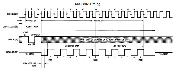
下图是ADC0832的时序图:
其中T-SetUp为250ns,由于使用的是51单片机,晶振11.0592MHz,机器周期比这个值大,可以不考虑,但为了防止出现异常,还是延时了两个机器周期。
注意在第11个时钟下降沿之后,DO上的电平既是MSB FIRST输出的最后一位,又是LSB FIRST输出的第一位。
以下是读取ADC0832的代码:
sbit CS_0832 = P1^1;
sbit CLK_0832 = P1^2;
sbit DO_0832 = P1^3;// DI、DO不同时有效,可共用一个接口
sbit DI_0832 = P1^2;
extern void _nop_ ( void );
#define pulse0832();
 _nop_();
_nop_();CLK_0832=1;
_nop_();
_nop_();
CLK_0832=0//把模拟电压值转换成8位二进制数并返回
unsigned char read0832()
{unsigned char i, ch = 0, ch1 = 0;CS_0832=0;// 片选,DO为高阻态
DI_0832=1;// 此处暂停
T-SetUp: 250ns (由pulse0832完成)pulse0832();// 第一个脉冲,起始位,DI置高
DI_0832=1;pulse0832();// 第二个脉冲,DI=1表示双通道单极性输入
DI_0832=1;pulse0832();// 第三个脉冲,DI=1表示选择通道1
(CH2)// 51单片机为准双向IO口:应先写入1再读取
DI_0832=1;// MSB FIRST DATAfor(i = 0; i < 8; ++i)
{pulse0832();ch <<= 1;IF(DO_0832==1)ch |= 0x01;}
// MSB FIRST输出的最后一位与LSB FIRST输出的第一位是在同一个时钟下降沿之后,故此处先执行读取,后执行pulse
LSB FIRST DATAfor(i = 0; i < 8; ++i) {ch1 >>= 1;
if(DO_0832==1)ch1 |= 0x80;pulse0832();}
CS_0832=1;// 取消片选,一个转换周期结束
return (ch==ch1) ? ch : 0;// 返回转换结果}
发挥结果给数码管0x23就是显示32,以16进制显示两位数,因为我们使用的是CD4511数码管译码器
同时我提供了ADC0804的程序,因为我实验室经常用ADC0804,但是价格上可能有点小贵
实现一次ADC转换主要包含下面三个过程:
1.启动转换:由图6中的上部“FIGURE 10A”可知,在CS信号为低电平的情况下,将WR引脚先由高电平变成低电平,经过至少tW(WR)I 延时后,再将WR引脚拉成高电平,即启动了一次AD转换。
注:ADC0804使用手册中给出了要正常启动AD转换WR的低电平保持时间tW(WR)I的最小值为100ns,即WR拉低后延时大于100ns即可以,具体做法可通过插入NOP指令或者调用delay()延时函数实现,不用太精确,只要估计插入的延时大于100ns即可。
2.延时等待转换结束:依然由图6中的上部“FIGURE 10A”可知,由拉低WR信号启动AD采样后,经过1到8个Tclk+INTERNAL Tc延时后,AD转换结束,因此,启动转换后必须加入一个延时以等待AD采样结束。
注:手册中给出了内部转换时间“INTERNAL Tc”的时间范围为62~73个始终周期,因此延时等待时间应该至少为8+73=81个时钟周期。比如,若R为150K, C为150pF,则时钟频率为Fclk=1/1.1RC=606KHz,因此时钟周期约为Tclk=1/Fclk=1.65us。所以该步骤至少应延时81*Tclk=133.65us. 具体做法可通过插入NOP指令或者调用delay()延时函数实现,不用太精确,只要估计插入的延时大于133.65us即可。
3.读取转换结果:由图6的下部“FIGURE 10B”可知,采样转换完毕后,在CS信号为低的前提下,将RD脚由高电平拉成低电平后,经过tACC的延时即可从DB脚读出有效的采样结果。
以下是ADC0804的程序:
#include<reg52.h>
#include <intrins.h>
#define uint unsigned int
#define uchar unsigned char
sbit cs=P3^5;
sbit rd=P3^6;
sbit wr=P3^7;
uint shu[10]={0x00,0x01,0x02,0x03,0x04,0x05,0x06,0x07,0x08,0x09},va1,va3,num=0;
uint shu1[10]={0x00,0x10,0x20,0x30,0x40,0x50,0x60,0x70,0x80,0x90};
float va2;
uint time[2]=0;
void delay(int x)
{ int i,j;
for(i=0;i<120;i++)
for(j=x;j<120;j++);
}
main()
{
TMOD=0x01;
TH0=(65536-917)/256;
TL0=(65536-917)%256;;
EA=1;
ET0=1;
TR0=1;
cs=0;
while(1){
_nop_();
wr = 0;
_nop_();
wr = 1;
delay(5);
_nop_();
rd = 1;
_nop_();
rd = 0;
_nop_();
va1 = P1;
rd = 1;
va2=((va1*1.0/255)*5.0);
va3=va2*100;
time[0]=va3/100;
time[1]=va3%100/10;
}}
void Tim() interrupt 1
{
TH0=(65536-917)/256;
TL0=(65536-917)%256;
num++;
if(num==10)
{
num=0;
P2=shu1[time[1]]|shu[time[0]];
}
}
测试部分准备的是直流稳压电源,先给芯片通20V电压,然后再测试输出电压是否正常,再一步一步调试,调试好之后就可以正式开始录制视频
可以说整个工程最难的地方就是在于调试
上图为测试流程
我最喜欢的阶段就是烤板
设置80摄氏度,烤它个30分钟,再继续测试,这是对PCB板的初步的严格测试
烤完之后有股淡淡的香味!
我们实验室有一台集成电路测试仪,可以测试芯片逻辑功能的好坏,同时还可以测试各个参数,型号为朗讯LK8810S,那我就拿它来测试ADC0804了。
根据ADC0804的时序逻辑可知
CS 先为低电平,WR 随后置低,经时间 tw(WR)L 后,WR 置高,
随后 AD 转换器被启动,并且在经过一段时间后,模数转换完成,转换结果存入数据锁存器,同时 INTR 自动变为低电平,通知单片机本次转换已结束。我们在实际单片机程序启动 A/D 转换时就要遵循上面的时序。但实际使用中,也可以不采用中断方式读取 A/D 转换数据,我们可以在启动 A/D 转换后,经过延时一段时间,直接取 A/D 转换数据结果,读取结束后再启动一次 A/D 转换,如此循环下去,AD 转换继续测试 2 组电压,第一组输入电压 1.65V 给 VIN+,判断得到的码值是否为 0x54,若码值正确,芯片功能正常,否则为不良品;第二组输入电压 3.32V 给 VIN+,判断得到的码值是否为 0xAC,若码值正确,芯片功能正常,否则为不良品。
上图为ADC0804的测试结果
I encountered various problems during the test, but through thinking and active modifications, I overcame the difficulties. I hope everyone will not give up easily if they encounter difficulties in the final step! !
First of all, for normal output voltage sampling display, many parameters need to be calibrated in order to achieve a certain accuracy. When the sampling value is converted into an actual voltage value, the result is directly related to the reference voltage of the ADC and the amplification ratio value of the hardware circuit. , although the value of the reference voltage has been given in the data sheet, there is a certain gap between the actual reference voltage and the data sheet. The amplification ratio of the signal conditioning circuit can also be calculated, but the tolerance of the components will make it inaccurate. Moreover, these two quantities are independent and not related, so a balance must be made between the two, and a relatively accurate value can be obtained based on multiple debugging calibrations. The specific values can be found in the attached program.
When debugging power factor detection, first observe whether the program can enter the external interrupt service routine. In fact, as long as the hardware is ready, there is no problem at all. In fact, this is also the case. The program can enter the interrupt service routine, but it cannot be seen on the monitor. As a result, only garbled characters are displayed, which can be seen later in the simulation.
Due to limited conditions, I only sample the input voltage and current, and the output voltage and current to calculate the actual power. The load uses a high-power sliding rheostat for easy adjustment.
The test results are very exciting. Most of the requirements in the question have been met. Because there is no power tester in the laboratory, the power can only be tested by preliminary measurement of input and output voltage and current, but it is also very satisfying! !
The competition has come to an end as of September 20th . This competition made me realize the importance of careful thinking on the field. I also need to think often in daily life and solve problems independently. For this project, I referred to a lot of information and designed the circuit myself. Until I finished the test, I was thinking alone. Thinking helped me learn how to deal with problems efficiently.
Next year, I will compete with friends from all over the country in the 2021 National College Student Electronic Design Competition.
At the same time, we would like to thank Lichuang for its strong support to our school laboratory! !
Our laboratory is a key laboratory for cultivating technical talents in Hunan Province, and is also a joint laboratory for Lichuang Electronic Design! !
I hope that Lichuangduo will organize similar competitions to enrich our knowledge and improve our professional quality! ! Thank you Lichuang! !


 京公网安备 11010802033920号

 AM70PDL127CDH85I