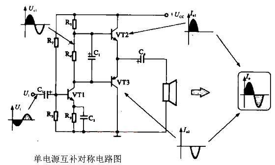
Use discrete components, capacitors, resistors and transistors to design a three-stage amplification circuit, and use push-pull output to increase the potential through resistor division to facilitate microcontroller ADC measurement. The stm32 microcontroller processes the data and draws the waveform through the LCD screen and displays each data. (1) The common emission of the first stage is used to ensure normal signal amplification. (2) The second stage common collector is directly coupled to the first stage, and the input and output impedances of the front and rear common emitter stages are adjusted so that the common emitter output of the latter stage can also have an amplification factor that meets the requirements. (3) The third-level common emission achieves top distortion and bottom distortion by adjusting the operating point. (4) The last stage is push-pull output, and the voltage output node is adjusted to 0-3.3V to adapt to the measurement range of the microcontroller.
Afterwards, the I/O port corresponding to channel 11 of the microcontroller ADC1 is PC1, and the ADC1_GPIO_Config() function is used to configure the PC1 port to collect voltage. We configure the ADC to trigger the ADC interrupt using a timer and configure the TIM2 in output PWM mode, triggered by the TIM2_CC2 input capture.We use STM32 4.3-inch LCD to display waveforms in real time. At the same time, pressing KEY0 and KEY2 can adjust the pulse width of the waveform. The keys KEY1 and KEY_UP can move the yellow cursor left and right to measure the voltage at a certain point of the waveform.

All reference designs on this site are sourced from major semiconductor manufacturers or collected online for learning and research. The copyright belongs to the semiconductor manufacturer or the original author. If you believe that the reference design of this site infringes upon your relevant rights and interests, please send us a rights notice. As a neutral platform service provider, we will take measures to delete the relevant content in accordance with relevant laws after receiving the relevant notice from the rights holder. Please send relevant notifications to email: bbs_service@eeworld.com.cn.
It is your responsibility to test the circuit yourself and determine its suitability for you. EEWorld will not be liable for direct, indirect, special, incidental, consequential or punitive damages arising from any cause or anything connected to any reference design used.
Supported by EEWorld Datasheet
EEWorld
subscription
account

EEWorld
service
account

Automotive
development
community

Robot
development
community

About Us Customer Service Contact Information Datasheet Sitemap LatestNews


Room 1530, 15th Floor, Building B,
No.18 Zhongguancun Street,
Haidian District,
Beijing, Postal Code: 100190
China
Telephone: 008610 8235 0740
 京公网安备 11010802033920号

 2200RAF60IPB2SA