Taishanpai CNC Shell and Panel:
The official Taishanpai CNC shell cannot be purchased through the 1 Yuan CNC promotion.
Bilibili: https://www.bilibili.com/video/BV1SZ4y1J7y6/?vd_source=74a9f6cb9a59140477fef67bbb0ec8ee
I designed a shell suitable for the 1 Yuan CNC promotion:
4 M3*20 screws,
3 M3 hand-tightening nuts, and some
thermal paste.
There are two versions of the CNC shell top:
this model has a frame,

and this model does not. The model with the frame


conflicts with the pin header and needs to be sanded.

01e8bb774a6c99c12874c3b817ab5bb2.mp4
20230918 Upper shell CNC v150.step
20230918 Upper Shell CNC v127.step
20230918 Lower Shell CNC v39.step
PDF_Taishanpai CNC Shell and Taishanpai Panel.zip
Altium_Taishanpai CNC Shell and Taishanpai Panel.zip
PADS_Taishanpai CNC Shell and Taishanpai Panel.zip
96145
efont_demo_10d2
The demo code for the Micropython module efont corresponds to the schematic diagram of the development board.
Efont demo (10.2-inch tri-color SD1677) schematic diagram ESP32-S3 (N8R2, N16R8) Sensors used:
- SHT30 temperature, humidity
- R8025T real-time clock
- FM11 NFC tag (not currently used)
1. For corresponding firmware source code, compilation, download, etc., please refer to the README.
2. For corresponding MicroPython scripts and tools, usage instructions, please refer to the README
. 3. The demo code for the distribution package is available on the cloud drive. The
code uses 4 pages: Switch | Configuration | Weather | Calendar. Below is a screenshot from the Windows simulator:


Configuration method, supports web and Bluetooth app (source code is in repository #2 for reference):

Bluetooth app configuration program, developed using Flutter, supports Windows and Android. Other platforms have not been tested.

The project code and tools reference many resources, which cannot all be listed. They are all described in the repository for reference.
The firmware and code are constantly being improved; discussion and exchange are welcome.
demo-video.mp4
PDF_efont_demo_10d2.zip
hsh102ew_1v11_sch.schdoc
PADS_efont_demo_10d2.zip
BOM_efont_demo_10d2.xlsx
96148
DM_MC02 H7 Development Board (with accessories)
A development board based on the STM32H723VGT6 microcontroller, suitable for RM and RC electronic design competitions.
1. DM_MC02 Introduction
Purchase Link:
Resource Link: (https://gitee.com/kit-miao/dm-mc02)

The DM_MC02 features multiple protections including reverse connection protection, overvoltage protection, and soft start. It has three FDCAN interfaces, two RS485 interfaces, one serial port, four servo interfaces, SBUS, USB, and interfaces for an OV5640 camera and LCD.
Currently, the open-source version is the interface board for the DM_MC02 H7 development board.
2. DM_MC02 Pin Labels

3. Resource Introduction

4. Circuit Design
H7 Baseboard Schematic Link: (https://gitee.com/kit-miao/dm-mc02/tree/master/Schematic)
Partial schematic diagram is shown below:

5. Software Examples
Here are the software examples for the DM_MC02.
H7 software example link: (https://gitee.com/kit-miao/dm-mc02/tree/master/examples)
The example directory is shown below:

6. BTB purchase link
BTB Taobao purchase link
7. Project log
(December 1, 2024, 11:45 AM) Created an open source project
PDF_DM_MC02 H7 Development Board (with accessories).zip
Altium_DM_MC02 H7 Development Board (with accessories).zip
PADS_DM_MC02 H7 Development Board (with accessories).zip
BOM_DM_MC02 H7 Development Board (with accessories).xlsx
96149
tda2003
Used as a pure power amplifier board, it lacks 5521 and 3.5mm jacks. Soldering tests showed normal sound with very low background noise, but resistor R3 overheated a bit. Due to laziness, I'll leave it as is and fix it later when I have more time.

Attention!!! The resistors in the PCB design are vertically soldered. Due to my limited experience, the 3D model and PCB pinouts do not match. These are modifications from a 0603 circuit. Please excuse the inconvenience.
PDF_tda2003.zip
Altium_tda2003.zip
PADS_tda2003.zip
BOM_tda2003.xlsx
96150
tea2025 redraw
I disassembled my old TEA2025 PCB from junior high school, redesigned and rebuilt the board, but omitted the DC port and 3.5mm audio jack.
November 19, 2024: Thanks to the comments section for pointing out the issue. I hadn't noticed the silkscreen markings on the capacitors on the circuit board. I've now adjusted them, increased the trace width, and fine-tuned the routing.
A 5521 female connector and indicator light circuit have been added to the power supply section. The indicator light circuit is very simple and can be omitted.
The modified board has not been tested and verified; please use it with caution.
Criticism and suggestions are welcome.
Feedback adjustments have been made, and a 330Ω resistor has been added to reduce gain.
PDF_tea2025 Redraw.zip
Altium_tea2025 redraw.zip
PADS_tea2025 redraw.zip
BOM_tea2025 redraw.xlsx
96151
RC522 Beta V4 NFC Card Reader (Function Verified)
This is a test board for an NFC card reader based on the RC522 microcontroller (card reading functionality verified). This project is based on the GPL 3.0 open-source license, hoping to save you time and effort.
Preface:
This is a test circuit board for an NFC card reader based on RC522 (functionality verified).
Since I've noticed that many people have publicly shared the RC522 circuit diagram, many details or principles haven't been clearly explained, I will try my best to analyze the entire circuit design to prevent pitfalls and help you avoid detours.
Main text:
The entire circuit diagram structure. Actually, when you look for the manufacturer's datasheet, they will also provide the corresponding diagram.
To help beginners, I will briefly explain the circuit on the left.
It's obvious that C1, C2, C4, C5, and C6 are all filters. So if your embedded device has power filtering, you can omit C1 & C2
, but it's not recommended to omit C4, C5, and C6 because these three capacitors filter internal noise from the chip (I won't go into details).
The REST pin in the circuit has a resistor and capacitor connected; this is actually for button debouncing. So if your circuit is directly connected to a microcontroller, you can consider omitting it.
As for the other components, they are auxiliary circuits inside the chip; you can just copy them directly.
Also, if you purchased the crystal oscillator I used, please remember that you cannot connect the two empty pins on either side of the crystal oscillator (it will short-circuit).
Okay, now for the main part:
I won't explain what LC resonance is in the antenna section , since you shouldn't even look at this if you don't understand such a basic principle.
Theoretically, antennas don't need to be this complex. According to simple resonance logic, only an inductor and a capacitor are needed, which is the so-called single-antenna first-stage resonant circuit.
However, in our circuit design, we made many design changes for stability. My circuit is a dual-antenna second-stage resonant circuit.
First, the communication frequency of the NFC protocol is 13.56MHz, and I have also put the frequency calculation formula for the LC circuit in the schematic diagram. In actual design, the values of the components themselves have a certain degree of error.
So I encourage you to use around 13.8MHz in the final calculation .
Actually, I feel that there is not much to say here, but in order to prevent beginners from understanding anything, I will talk about the various functions of the antenna components!
As can be seen from the schematic diagram: This dual-antenna circuit is symmetrical, so I will just talk about the components of the upper part: L1 and C11 constitute the first-stage resonant circuit.
It is best to use a simple wire-wound inductor for this group of L (I am not familiar with other inductors and may cause problems, so I can't guarantee it). Tips: This kind of inductor is now also available in surface mount packages.
As for C13 Essentially, it's about passing AC and blocking DC. If you don't understand, you can think of it as anti-interference. Recommended capacitor values are 20~100pF.
C15 & C18, together with the antenna, form a two-stage resonant circuit. Why two capacitors? Mainly for easier debugging and verification. You can use just one capacitor; it doesn't matter, you can calculate it yourself using the formula.
Regarding the coil, if you look at the PCB, you'll see I've drawn a PCB diagram. This is based on TI's Coil Master (a small free advertisement for them). Although it's not perfect, it works. If you're interested, you can draw it yourself.
Finally, there's the antenna wiring. Based on my verification, grounding the middle antenna does indeed provide more stability with dual antennas.
Okay, that's the design guide. Now, let's briefly talk about the debugging guide:
I guess you encountered a bug in your design and came here hoping for luck, so you're in luck!
First, you need an oscilloscope.
Connect the oscilloscope probe and clips directly to both ends of the antenna.
If it's a normal circuit, you should be able to read a perfect sine wave signal
around 13.56MHz with a voltage amplitude (Vpp) roughly within 3V.
If it's abnormal... Please check if your soldering and crystal oscillator are working properly.
Then, if there's a sine wave but the microcontroller can't read the data,
first ensure your code is correct,
then check the VSS and VDD connections of the chip
to ensure they are normal, and finally, ensure there are no cold solder joints.
If it still doesn't work after all this, then the problem lies with you (don't be tempted to buy cheap, low-quality chips and components)
. Okay, that's all I wanted to say.
I hope you avoid some pitfalls!
PDF_RC522 Beta V4 NFC Card Reader (Verified Functionality).zip
Altium_RC522 Beta V4 NFC Card Reader (Function Verified).zip
PADS_RC522 Beta V4 NFC Card Reader (Function Verified).zip
BOM_RC522 Beta V4 NFC Card Reader (Function Verified).xlsx
96152
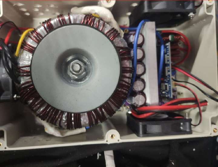
Power frequency sine wave inverter
The EGS002-based industrial frequency inverter module has an adjustable output from 100V to 200V, a fixed frequency of 50Hz, and a maximum power of 300W (with a fan; the toroidal transformer's maximum power is only 220W overload).
Please use the attached PCB for prototyping!
The DC-DC inverter uses 220V AC power; the input voltage should ideally not exceed 36V. The chip's withstand voltage is 40V, and the capacitor's withstand voltage must be greater than the operating voltage.
You will need to drill holes for the heatsink yourself.
I recommend the SKD502 MOSFET; it seems to offer the best value in the TO220 package, mainly because it's easy to drive.
An EMI inductor is connected to the output; you can short it if not needed.
I used a cheap AC meter from Taobao (around 2 RMB), which seems adequate.
The control module uses EG002: https://item.taobao.com/item.htm?spm=a21n57.1.0.0.6081523cXXl1Ul&id=529512690892&ns=1&abbucket=13#detail
Heatsink link: https://detail.tmall.com/item.htm?abbucket=13&id=622017593211&ns=1&spm=a21n57.1.0.0.6081523cXXl1Ul&skuId=4570933003342
MOS link: https://item.taobao.com/item.htm?spm=a21n57.1.0.0.6081523cXXl1Ul&id=670316290351&ns=1&abbucket=13#detail
Header link: https://item.taobao.com/item.htm?spm=a21n57.1.0.0.6081523cXXl1Ul&id=45094165395&ns=1&abbucket=13#detail

ALPHA EG8010 DC-AC C01.zip
Wiring diagram.png
PDF_Power Frequency Sine Wave Inverter.zip
Altium_Power Frequency Sine Wave Inverter.zip
PADS_Power Frequency Sine Wave Inverter.zip
BOM_Power Frequency Sine Wave Inverter.xlsx
96153
electronic


 京公网安备 11010802033920号

 CD-700-LAC-GEB-77.760


