ncDmyaM8a

Training Course - Precision Instrument Amplifier

 
Overview
Project Introduction:
This project is the first lesson in the Lichuang training program for first-year university students. Building upon the basic knowledge of operational amplifiers taught in the previous lesson, it further explains the circuitry of precision instrumentation amplifiers and guides students in designing their application circuits, enabling them to apply their knowledge in practice.
Project Functions:
This precision instrumentation amplifier features ultra-low cost, ease of use, and wide applicability. Its basic function is to serve as the analog front-end for simple oscilloscopes and multimeters. It features high input impedance, differential input, high-precision gain, and adjustable bias output. Furthermore, the use of dual potentiometers allows for both coarse and fine adjustment, enabling convenient and precise gain control. Compared to traditional three-op-amp instrumentation amplifiers, an additional op-amp is used as a reference voltage buffer because this conveniently provides the bias voltage required by common sampling circuits such as subsequent ADCs.
Project Parameters
Core IC: TL084 Operational Amplifier: This is a classic, nationally used teaching-grade op-amp for electrical and electronic experiments. It is a high-input-impedance, high-slew-rate op-amp based on FET input-stage technology, with a very low offset voltage of only 3mV (datasheet data). It has almost no input compensation current and is unity-gain stable. One chip contains four op-amps, making it ideal for use as a three-op-amp instrumentation amplifier plus a reference voltage buffer.
Peripheral Circuit: A basic three-op-amp instrumentation amplifier topology. The gain adjustment uses a 200-ohm gain-limiting resistor plus two 3386 single-turn potentiometers, which can be easily adjusted with a screwdriver. The resistor values ​​are 1kΩ and 10kΩ, therefore, the lower gain limit is 2.8, and the upper gain is close to 100, providing a wide adjustable range while allowing for easy and precise adjustment.
Principle Analysis (Hardware Description)
: The principle of the three op-amp instrumentation amplifier is as follows: First, two op-amps form a fully differential amplifier. The amplification factor is easy to calculate: First, set a virtual short equation for each op-amp, and you can get
Vo+-Vo-=(1+20kΩ/R3)*(Vi+-Vi-).
Then, the last op-amp is a differential-to-single-ended circuit.
Precautions:
If you want to test the waveform of mains power, you should add at least a 40dB attenuator in the preamp stage. This can be achieved simply by using a 1MΩ resistor and a 10kΩ resistor for voltage division. Because this part of the circuit involves high voltage, it should be connected to an external board to prevent interference, and copper should not be laid (you can directly solder a resistor to the point).
Additionally, if you want to modify it into a current measurement module, you should add a 0.1Ω precision sampling resistor at the high-impedance input terminal, connected across the differential input terminal.
The assembly process
begins by applying solder paste to the surface mount pads, followed by the surface mount resistors and capacitors, which are then soldered using a hot air gun. Next, the through-hole IC sockets, pin headers, and potentiometers are soldered. Finally, the TL084 is inserted (note the orientation). Powering on and testing is then possible. First, connect the power supply and check for overcurrent (to prevent short circuits). If no overcurrent occurs, apply a test signal (typically a 1kHz, 100mVpp sine wave) to check the output waveform for normality. Adjust the gain to see if it's flexible and the bias is easy to adjust.
Afterward, place it in a non-common-ground circuit with a large common-mode voltage to check for a high common-mode rejection ratio. [
Image of the actual component]
PDF Training Course - Precision Instrument Amplifier.zip
Altium Training Course - Precision Instrument Amplifier.zip
PADS Training Course - Precision Instrument Amplifier.zip
BOM_Training Course - Precision Instrument Amplifier.xlsx
91855
Voron0.2_Network Cable Hub
Voron 0.2_ Official Mini SB Hot-End and Noctua Head Dual 4010 Fan Hot-End Network Cable Hub
Voron0.2_ Official Mini SB Hothead and Cat Head Dual 4010 Fan Hothead voron/V0/Dragon_Burner at main · chirpy2605/voron · GitHub Network Cable Hub
 
Mini SB Connector was the first one I made and forgot to take a picture of it. The power supply board is universal.
 
BOM:
1 straight-through network port (RJ45 5224 dual port)
, 1 right-angle network port (RJ45 59-1*2 dual port)
, 1 straight-through 4p XH2.54,
1 right-angle 4p XH2.54
, 12 straight-through
2p XH2.54, 2 right-angle 2p XH2.54 (optional, two spare ports) .
-
The circuit board securing the power compartment requires two M3*6+6 nylon posts (copper posts are also acceptable, longer or shorter is fine. Ideally, M3*6+3, but if +3 posts are unavailable, +6 posts can be purchased and shortened; leaving them uncut won't affect anything). Two M3 screws are also needed.
 
The small board at the top of the power compartment needs to be drilled and replaced; the STP file has been uploaded.
Battery Pack Board.stp
PDF_Voron0.2_Network Cable Hub.zip
Altium_Voron0.2_Network Cable Hub.zip
PADS_Voron0.2_Network Cable Hub.zip
91856
GPW series micro switch
GPW Hot-swappable Miniature Board
Because I accidentally burned the PCB/A pads while modifying the microswitch for hot-swapping due to double-clicking, and buying a replacement on Taobao would cost almost ten yuan, I decided to start this project.
Future Logitech/Razer microswitch mini-board projects will be updated on this account.
Friendly reminder: When boarding GPW mini-boards, please select 0.8mm. 
GPW version 1.3 is still under testing. Version
1.31 has been modified. (Continued from above, FPC board testing confirmed; some hole spacing still has deviations and needs correction.
 
Updates will be sporadic and I'm just being lazy.)
PDF_GPW Series Microswitch Board Logi.zip
Altium_GPW series microswitches Logi.zip
PADS_GPW series micro switches Logitech Logi.zip
PDF_GPW Series Microswitch Board Logi.zip
Altium_GPW series microswitches Logi.zip
PADS_GPW series micro switches Logitech Logi.zip
91857
ESP32_C3_LCDKit
Compatible with Espressif's LCDKit project. The design has been changed to a watch-like round shape, and the screen has been upgraded to a more aesthetically pleasing touchscreen.

![01-LCDKit project.png]
PDF_ESP32_C3_LCDKit.zip
Altium_ESP32_C3_LCDKit.zip
PADS_ESP32_C3_LCDKit.zip
BOM_ESP32_C3_LCDKit.xlsx
91860
MoriPower-GBA Lithium-ion Battery Charge/Discharge Module (AXP209 Version)
 The MoriPower-GBA lithium battery charge/discharge module (AXP209 version)
 
uses the AXP209 as the PMIC, supports ordinary polymer soft-pack lithium batteries, and outputs 3.3V to the GBA. When
the battery voltage is below 3.5V, the low battery indicator D2 will light up; during charging, the charging indicator D1 will light up.
Charging supports a C-to-C connector with a 5V input.
 
Note:
1. The 30mΩ resistor in the charging circuit cannot be replaced with a 0Ω resistor, as this will cause overheating during charging.
2. The inductor's rated current must be above 1A.
3. If the charging indicator flashes once per second during charging, it indicates a charging malfunction; resolder the AXP209, as this is caused by a lack of proper grounding at pin 37.
PDF_MoriPower-GBA Lithium Battery Charge/Discharge Module (AXP209 Version).zip
Altium_MoriPower-GBA Lithium Battery Charge/Discharge Module (AXP209 Version).zip
PADS_MoriPower-GBA Lithium Battery Charge/Discharge Module (AXP209 Version).zip
BOM_MoriPower-GBA Lithium Battery Charge/Discharge Module (AXP209 Version).xlsx
91861
Sky Star Expansion Board
I. Project Introduction
This is a SkyStar expansion board developed based on LCSC SkyStar, compatible with three versions of SkyStar (STM32/GD32/HC32).
II. Onboard Functions
2.1 Digital Tube
2.2 I2C Display
2.3 Vibration Motor 2.4
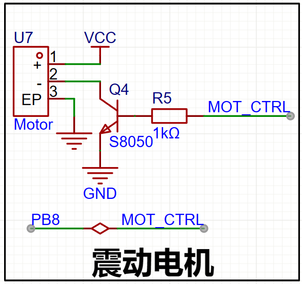
Buzzer
2.5 RTC Clock
2.6 Independent Buttons
2.7 Matrix Buttons
2.8 Potentiometer
2.9 Thermistor
2.10 Temperature and Humidity Sensor
2.11 SPI Display
90c80dd00a68e902d5464adfd55eb682.mp4
PDF_SkyStar Extension Board.zip
Altium_SkyStar Expansion Board.zip
PADS_SkyStar Expansion Board.zip
BOM_SkyStar Expansion Board.xlsx
91862
RTL8305NB-CG 5-port 100Mbps switch
This low-cost 5-port switch based on the 8305nb is simple to solder and inexpensive, making it suitable for beginners.
Soldering Difficulty: Easy
Soldering Time: 15 min, 20-35 min for beginners
Component Cost:
RJ45 1X5 socket, all plastic 0.75r, half-package 1r, full package 3-4r;
RTL8305NB 2.5-3r;
H1102NL 0.4-0.5r;
other components 3r;
total 8.5-11r.
Test Diagram: Tested using GT01F4GA board and Itestatt software, no packet loss after 3 days of full load testing.
PDF_RTL8305NB-CG 5-Port 100Mbps Switch.zip
Altium_RTL8305NB-CG 5-port 100Mbps switch.zip
PADS_RTL8305NB-CG 5-Port 100Mbps Switch.zip
BOM_RTL8305NB-CG 5-Port 100Mbps Switch.xlsx
91864
The Super Spark Source for [2023 Electronic Engineering Contest Problem A] and [Switching Power Supplies]
This is an open-source project that includes [2021 Problem C], [2022 Problem A], [2023 Problem A], [BOOST], [BUCK-BOOST], and [inverter circuit].
This project
introduction
includes the following parts:
1. Schematic diagram of a three-port DC-DC converter (Problem C of the 2021 National Electronic Design Contest)
; 2. Schematic diagram of a single-phase AC electronic load (Problem A of the 2022 National Electronic Design Contest)
; 3. BOOST circuit;
4. BUCK-BOOST circuit;
5. DC-AC converter;
6. Schematic diagram of a single-phase inverter parallel operation system (Problem A of the 2023 National Electronic Design Contest).
Why only schematic diagrams? Because during the contest, things were rushed; PCB layouts were repeatedly drawn and deleted, and eventually lost. So please bear with it.
Note: When opening the project, first look at the readme. The program was written by my teammate, so there is no actual code! No code! No code! But there is a program logic!
==============================2023 Electrical Engineering Contest A Project Introduction================================
This project has not completed the advanced part, only the basic requirements have been met.
I. Project Requirements
Let's review the basic requirements of the 2023 Electrical Engineering Contest A Project.
1. Basic Requirements
(1) Disconnect S2 and close S1, and use only inverter 1 to supply power to RL. When the effective value of the output voltage Uo is 24V±0.2V and the frequency fo is 50Hz±0.2Hz, the effective value of the output current Io is 2A.
(2) Under the working conditions of basic requirement (1), the total harmonic distortion (THD) of the output AC voltage is not greater than 2%.
(3) Under the working conditions of basic requirement (1), the efficiency of inverter 1 is not less than 88%.
(4) With S2 open and S1 closed, only inverter 1 supplies power to the load. When Io varies between 0A and 2A, the load regulation rate SI1 ≤ 0.2%.
II. Overall Design Block Diagram and Description
III. Hardware Circuit Description
IV. Software Part and Output Results
Software Part:
(1) Program Function Description
The microcontroller is made into an automatically adjustable SPWM wave generator that can stably output voltage and maintain communication with the specified circuit.
(2) Program Design Ideas
To complete the design of the single-phase inverter parallel operation system in this paper, not only hardware design is required, but also software design. In order to realize the various functions of the microcontroller, the compilation of software programs is indispensable. This system uses C language to write programs and Keil5 DMK as the integrated development environment.
Dividing a sine wave with F=50Hz and T=20ms into 200 equal parts, we know that each part is 1/(200*50)=0.1ms=100us.
Therefore, by modifying the width of the PWM wave every 0.1ms, a sine wave similar to an SPWM wave can be output, as shown in the figure below.
The microcontroller configuration is as follows:
Set the total system clock frequency to 48MHz;
use advanced timer TIM1 to output a 20kHz dual-channel complementary PWM wave with dead time as the carrier of the SPWM;
use general-purpose timer TIM2 to perform time-division processing of the program, and run the corresponding program when the time reaches the corresponding time to ensure the program runs in an orderly manner;
use general-purpose timer TIM3 to change the width of the PWM wave every 0.1ms as the fundamental wave of the SPWM, and read the ADC value and feed it back to the microcontroller for peak adjustment of the SPWM wave;
use ADC1 group, and use the 4 ADC channels in the group to read the values ​​of voltage, current, etc.
Output Results:
V. My Own Notes
=== ... =============================BUCK-BOOST Circuit Description= ...


PDF_【2023 Electronic Engineering Contest A Problem】and 【Switching Power Supply】Super Spark Source.zip
Altium_【2023 Electronic Engineering Contest A Problem】and 【Switching Power Supply】Super Spark Source.zip
PADS_【2023 Electronic Engineering Contest A Problem】and 【Switching Power Supply】Super Spark Source.zip
BOM_【2023 Electronic Engineering Contest A Problem】and 【Switching Power Supply】Super Spark Source.xlsx
91865
51 microcontroller minimum system
The microcontroller minimum system board based on the STC89C52RC is easy to replicate.
Project Inspiration:
I had been using a Puzhong development board to learn microcontrollers, but after a while, I felt that some functions were not comprehensive enough. Therefore, I designed my own microcontroller minimum system board and then connected external circuitry for use.
The circuit design
is simple in principle, using a CH340C to communicate with the microcontroller, and downloading requires only a T-Pic cable.
Replicating the project
as a whole is not difficult. However, care must be taken when soldering the T-Pic; because the mounting holes for the T-Pic are relatively small, it's crucial to ensure the T-Pic is completely secured during soldering, otherwise, the T-Pic port might become dislodged when connecting it later.
BOM_Board1_Schematic1_2024-09-24.xlsx
IMG_2673.HEIC.JPG
PDF_51 Microcontroller Minimum System.zip
Altium_51 Microcontroller Minimum System.zip
PADS_51 Microcontroller Minimum System.zip
BOM_51 Microcontroller Minimum System.xlsx
91866
electronic
参考设计图片
×
 
 
Search Datasheet?

Supported by EEWorld Datasheet

Forum More
Update:2026-03-27 15:48:50

EEWorld
subscription
account

EEWorld
service
account

Automotive
development
community

Robot
development
community

About Us Customer Service Contact Information Datasheet Sitemap LatestNews


Room 1530, 15th Floor, Building B, No.18 Zhongguancun Street, Haidian District, Beijing, Postal Code: 100190 China Telephone: 008610 8235 0740

Copyright © 2005-2024 EEWORLD.com.cn, Inc. All rights reserved 京ICP证060456号 京ICP备10001474号-1 电信业务审批[2006]字第258号函 京公网安备 11010802033920号