The miniaturized network port using JST-GHS functions identically to a transformer-equipped RJ-45 connector, and its use in space-constrained network port connection scenarios
has been proven successful.
A USB 2.0 1-to-4 expansion dock, constructed with a two-layer PCB, achieved a stable speed of 40 Mbps when tested with an external crystal oscillator.
This is a minimum system board based on the Allwinner H616 main controller.
Seeing many H616 development boards on the open-source forum, I decided to build my own minimal system board. I burned in a system ported by @iMrX from the group. The board has two USB 2.0 host ports, one UART, and one BTB2x10 SPI LCD interface. The LCD driver hasn't been ported yet. The sample board uses a 512MB Hynix DDR3 memory chip. There's no wired network connection, but the onboard Wi-Fi module can be used for internet access. The tested functions are: HDMI output works normally, but flickering occurs at 3440x2160 resolution, likely due to insufficient memory; lower resolutions output normally. The two USB ports communicate normally, and the Wi-Fi module works correctly.
This document describes how to implement a HomeKit thermo-hygrometer using an ESP32C3 microcontroller, and how to use a small TV SD2 casing to directly display the clock and temperature/humidity.
1. Function Introduction:
This project is inspired by the SD2 mini TV. The main controller is an ESP32C3, the screen is a 1.54-inch TFT color screen, and the temperature sensor is an SHT30.
Basic Functions:
1- Displays time, Wi-Fi connection, and battery level.
2- Displays temperature and humidity.
3- Directly connects to HomeKit, allowing users to view temperature and humidity via their mobile phones.
2. Hardware Description:
1- Powered by a 5V Type-C connector, it can be powered directly by a 1S lithium battery. A battery level icon is displayed, and a simple voltage indicator shows the battery level.
2- Due to HomeKit connectivity requirements and the high screen temperature, the temperature sensor is externally connected.
3- The casing is directly from the SD2 (https://oshwhub.com/Q21182889/esp-xiao-dian-shi), with a manual modification to add a sleeve to allow the temperature sensor wires to pass through. Glue is required.
4- The PCB board is 1.2mm thick.
3. Software Description:
1- This software is developed using ESP-IDF and comes with the ESP-HomeKit SDK to implement Apple HomeKit.
2- The graphical interface is implemented using LVGL.
3- The software is downloaded directly to 0x0000 using Espressif's flash_download_tool.
4- Thermometer_v1.0.0.bin will not turn off the screen. 5- Thermometer_v1.0.1.bin
automatically turns off the screen at 9:30 PM and automatically turns it on at 6:30 AM.
6- Supports over-the-air (OTA) pairing. It can be used with the Espressif App or the WeChat AirKiss (follow Espressif Systems' official WeChat account). It will automatically enter the pairing process after changing the Wi-Fi environment or router password. A Wi-Fi icon will appear after a successful network connection. Pairing will fail if the distance to the router is too far.
7- The network will automatically calibrate the time after a successful connection.
8- HomeKit connection: No code or cannot scan? Enter pairing code 11122333 to connect.
4. Finished Product and Effects:


iOS 12 Effects -

Home Assistant History

BOM.xlsx
Gerber ver1.2.zip
Schematic diagram.pdf
thermometer_v1.0.0.bin
thermometer_v1.0.1.bin
PDF_ESP32C3 Homekit Temperature and Humidity Astronaut Clock.zip
Altium_ESP32C3 HomeKit Temperature and Humidity Astronaut Clock.zip
PADS_ESP32C3 Homekit Temperature and Humidity Astronaut Clock.zip
BOM_ESP32C3 HomeKit Temperature and Humidity Astronaut Clock.xlsx
95031
Self-made DAP_Link (based on LCSC)
This is a modification of the JLCPCB DAP-Link, adding a 3.3V output. Users can freely choose between 3.3V and 5V output.
DAP-Link Based on CH552G (Modified from LCSC)
: This project modifies and
creates a
custom DAP-Link downloader (LCSC modified version) based on the JLCSC DAP-Link. [Video link:
https://www.bilibili.com/video/BV1ix4y187Ar](https://www.bilibili.com/video/BV1ix4y187Ar
) [
Image of the actual product] (https://www.bilibili.com/video/BV1ix4y187Ar) [


Instructions for use:
Modified from the JLCSC DAP-Link, adding a 3.3V output. 3.3V and 5V outputs can be freely selected. This DAP-Link has a pin header interface and an SH1.0 1x6pin reverse ribbon cable interface. The SH1.0 1x6pin reverse ribbon cable interface allows selection of the output voltage as 3.3V or 5V.
] ( https://www.bilibili.com/video/BV1ix4y187Ar

) For firmware download instructions, please refer to LCSC: LSPIClink: LCSC Liangshanpai Development Board with DAPlink using CH552G as the programmer controller. LCSC Development Board Official Website: lckfb.com (gitee.com)


Firmware.zip
Firmware download software.zip
PDF_DIY DAP_Link (based on Lichuang).zip
Altium_DIY DAP_Link (based on Lichuang).zip
PADS_DIY DAP_Link (based on LICK).zip
BOM_Custom-made DAP_Link (based on LICK).xlsx
95032
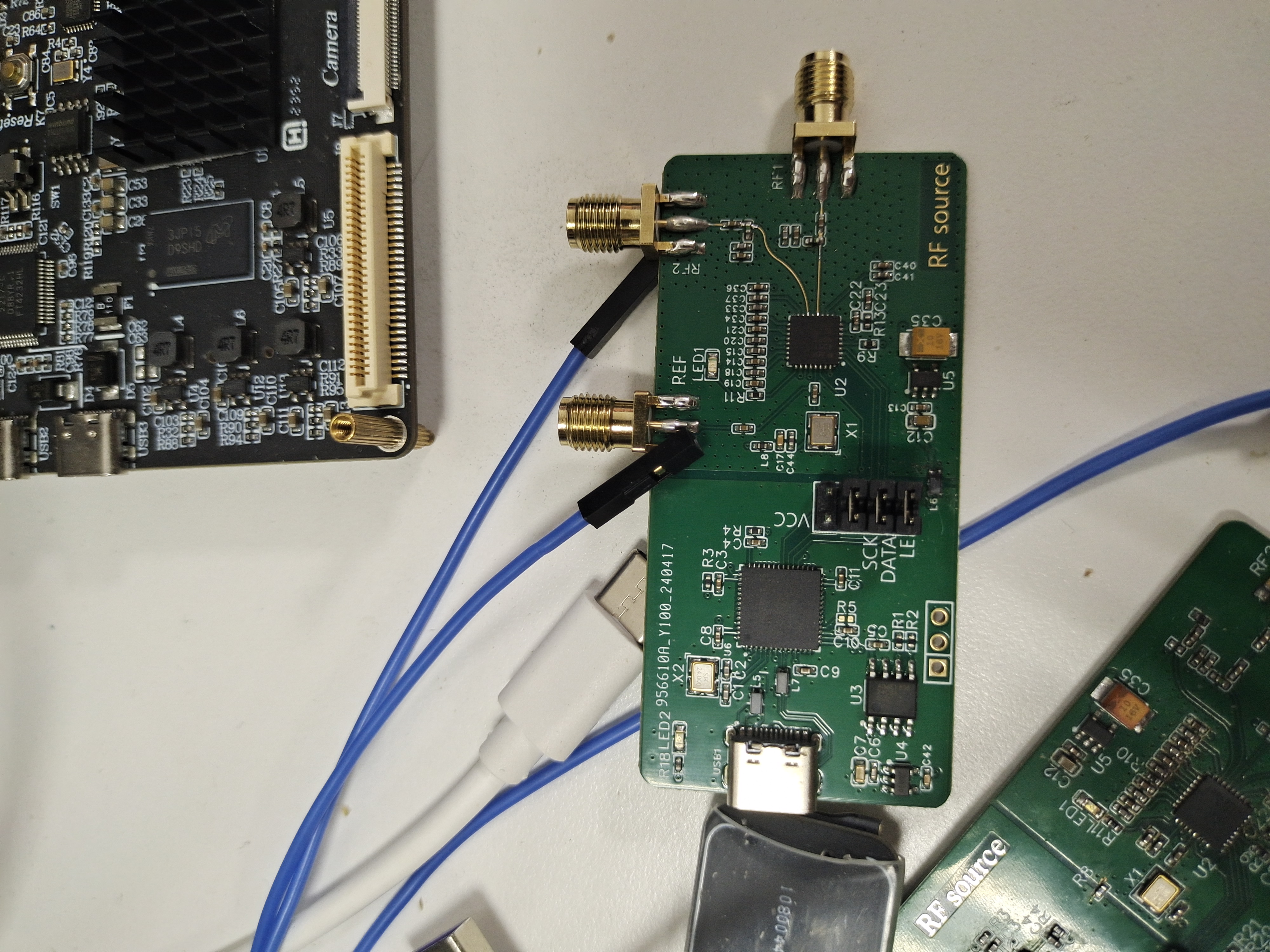
ADF4351 RF signal generator
Using the CY7C68013A as the main controller and the ADF4351 phase-locked loop (PLL), it can provide RF signal sources from 35MHz to 4.4GHz, is compatible with ADI's official host computer software, and can directly control the output.
This project
uses the CY7C68013A as the main controller and the ADF4351 phase-locked loop (PLL) as the primary loop unit. It provides RF signals from 35MHz to 4.4GHz, is compatible with ADI's official host computer software, and can directly control the output under
the open-source license
GPL 3.0.
Project-related functions
can be developed by writing your own program, or the firmware can be burned to the EEPROM via the provided binaries and used directly with ADI's official host computer software.
After flashing the firmware, the computer will recognize it as an ADF4xxx USB Adapter Board. If there is no firmware in the EEPROM, it will be recognized as a serial device (exclamation mark) .

Project Attributes:
This project is being publicly disclosed for the first time and is my original work. This project has not won any awards in other competitions.
The project
is complete with ADIsimPLL simulation
of the design principles
. The files are attached:


ADF4351 functional block diagram,

software description, and
BIN file. Write the following values sequentially from address 0x00 :
0xc0, 0x56, 0x04 , 0x03, 0xb4, 0x00, 0x00, 0x00. I'm using a Linux development board with i2ctools, so no programs are used. The official ADF435x host computer is shown in the physical demonstration (1GHz, 2.6GHz, 1.6GHz) . Design considerations (cy7c68013a): If the computer doesn't respond or displays an "unrecognized device" message, the chip is not properly soldered. There are three jumpers on the header; the top one is for VCC and GND. Do not short-circuit them. Other demo videos: Demo videos can be uploaded as attachments. Attachments can only be 50MB in size. Files larger than 50MB can be hosted on other cloud storage services or video websites; simply include the link here. Project attachments: Entries participating in the event must upload the relevant program attachments to an open-source platform or personal code storage cloud. Attachments can be uploaded up to a maximum of 50MB (please do not upload to the LCSC workspace, as there are limitations).


ADF4351-1.pll
video_20240427_185216.mp4
firmware.txt
PDF_ADF4351 RF signal source.zip
Altium_ADF4351 RF signal generator.zip
PADS_ADF4351 RF signal generator.zip
BOM_ADF4351 RF Signal Generator.xlsx
95033
FPC Watches
Based on the CH583M OLED watch, it uses FPC material and is easy to fold and wear on the wrist.
Main controller: CH583M, 60MHz main frequency, 512K flash, 32K ram, with Bluetooth 5.0 BLE;
Screen: OLED 12864, 4-wire SPI interface
; Gyroscope: ICM20608, SPI & IIC;
Independent buttons: 2
; ADC: NTC temperature measurement, battery voltage measurement;
Development environment: Mount River System


MAH00626.MP4
PDF_FPC Watch.zip
Altium_FPC watch.zip
PADS_FPC watch.zip
BOM_FPC watch.xlsx
95034
electronic


 3. Referring to the datasheet, an LDO module can be used for main controller power supply to improve stability. The CJA1117-3V3 LDO is an option.
  4. Both the light strip and onboard power are supplied via a TYPE-C 16-pin connector. The WCH CH340N module can be used for program download. Pressing the reset and download buttons will put the ESP-12F into download mode.


 京公网安备 11010802033920号

 CC0603JX7R110M


