iQmYbP

Naxi Da - Painting

 
Overview
Choose your preferred color; black or green solder mask is fine. Select the board thickness as needed (thinner is better). Use full-surface copper plating and solder mask openings for a smoother and more refined finish. The actual product will look much better than the photos, and it has a light effect (not really).
Naxida physical simulation image.png
PDF_Nasita-painting.zip
Altium_Nasita-painting.zip
PADS_Nasida-Painting.zip
96060
2.0A male to female USB-min
The USB 2.0 Type-C to Type-C adapter has differential wiring, works perfectly in both directions, and transmits and supplies power normally. Nothing else to say. The actual product is shown below.
This is a USB 2.0 Type-C to Type-C adapter with differential wiring. It works perfectly in both directions, with normal transmission and power supply. Nothing else to say. The actual product is shown below.
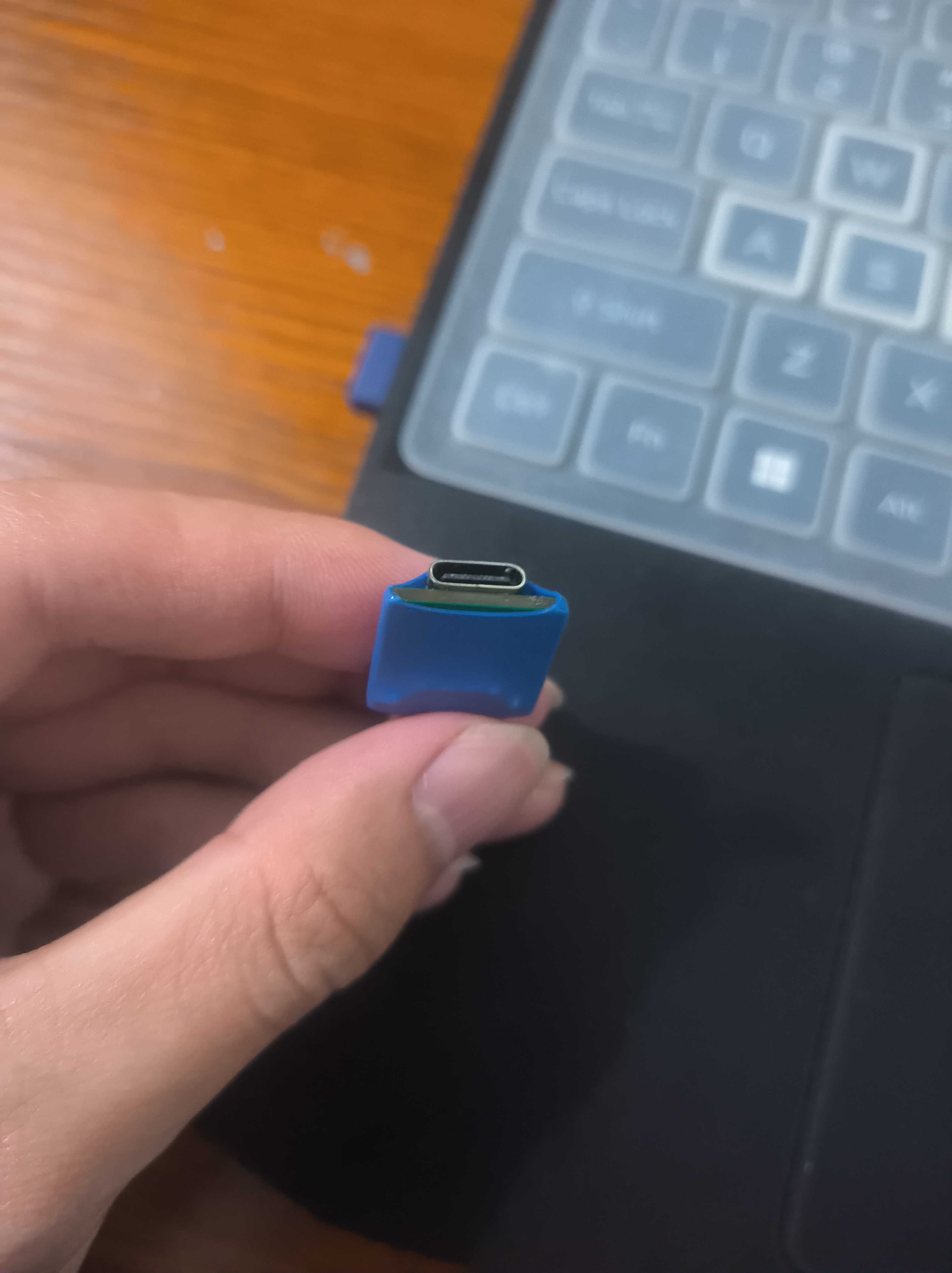
The 16-pin Type-C interface isn't particularly difficult to solder; with proper temperature adjustment, drag soldering can achieve a smooth finish in one go. Beginners can try using solder paste with its included flux for a more comfortable experience. Use a clip to hold the connector in place while soldering, and release it afterward. Solder the four retaining pins. If using solder paste, the retaining pins need to be soldered on both sides, otherwise they will be very weak.
Note that you should solder the Type-C pin first, then the Type-A pin, otherwise there will be a conflict and nowhere to place the soldering iron. (The LEDs and Denso components are just for fun; add them as needed.)
 
USB 2.0 physical simulation diagram 1.png
USB 2.0 physical simulation image.png
PDF_2.0A Male to Female USB-Min.zip
Altium_2.0A male to female USB-min.zip
PADS_2.0A male to female USB-min.zip
BOM_2.0A male to female USB-min.xlsx
96061
8038 Multifunctional Signal Generator
Course design: Multifunctional signal generator (analog electronics)
Design Task Analysis
: Design a generator capable of producing sine waves, square waves, triangle waves, and single-pulse signals, with the following requirements:
• Output frequency f: continuously adjustable from 20Hz to 5kHz for sine, square, and triangle waves.
• Output amplitude: 5V single-pulse signal.
• Output sine wave amplitude Vo: adjustable from 0 to 5V, with a waveform nonlinearity distortion coefficient y ≤ 5%.
• Output triangle wave amplitude Vo: adjustable from 0 to 5V.
• Output square wave amplitude: adjustable from 0 to 12V.
• Single-pulse output function. (
 
 
At the time, I wrote these to reach the word count.
When I saw the course design requirements, my first reaction was to use a PCB. Considering the numerous and complex wires on a breadboard, it was better to use a more advanced method: wiring on a two-layer board.) Then came the schematic drawing. The reference schematic in the chip datasheet had some minor issues, such as resistor values, operational amplifier parameters, a missing negative power supply for the function chip, difficulty finding a single-pole triple-throw switch, and the absence of a step switch, etc. The above issues were addressed one by one during the schematic drawing process. This included correcting faulty lines, adjusting incorrect values, and replacing switches. After simulation, the schematic was confirmed to be error-free (especially the NAND gate section). Following this, the layout was moved to the next step. Considering the limited number of components, all were placed on a single side. The PCB was made larger, resulting in a neat, flat, and easy-to-operate layout. Considering the time-sensitive nature of PCBs, through-hole components were chosen. This facilitates soldering, and if a PCB isn't ready in time, a breadboard can be used as a lower-level replacement. This also helps the team understand the circuit. I prefer a more symmetrical layout, and considering the need for a layout close to the schematic for easier understanding, I made minor adjustments to the function section based on the schematic to maintain its aesthetic symmetry while keeping the relative positions of the smaller parts unchanged. For the step section, since the chip is a quad NAND gate integrated circuit, I simply connected the wires directly, then arranged the resistors and the replacement switches symmetrically horizontally. Then came the complex wiring. The main considerations are: on a single layer, lines must not overlap; using a double layer concentrates the lines, facilitating separate routing for the top and bottom layers; routing should be optimized to eliminate high-frequency signal interference; considering the characteristic of through-hole components connecting the top and bottom layers, unlike surface mount components, the routing must fully consider the top and bottom layers. Then there are considerations such as trace spacing and thickness. Finally, add appropriate and necessary silkscreen text instructions. Soldering through-hole components is relatively simple and will not be described in detail here. Although the overall layout is relatively open, attention should be paid to the soldering order in relatively concentrated areas to avoid component interference. Pay attention to soldering quality. Testing should proceed without problems.
 
 
Analog circuit physical simulation diagram.png
PDF_8038 Multifunctional Signal Generator.zip
Altium_8038 Multifunctional Signal Generator.zip
PADS_8038 Multifunctional Signal Generator.zip
BOM_8038 Multifunctional Signal Generator.xlsx
96062
CH9328—Serial Port to HID Module
Serial to HID module, about the size of a coin!
Schematic Design Instructions
Schematic Reference Manual Example Circuit Design (The example circuit in the manual is shown below)
(The above is the reference circuit from the manual; all circuits below are for this project)
1. To save space, all resistors, capacitors, and LEDs are packaged in 0402 packages.
2. D1 and D2 in the diagram below have been removed in this project.
3. Because this module only needs to receive data, which is then converted by the chip and connected to the computer via USB, only the RX port of the UART interface is provided.
4. This module is a small test board designed to test all modes, hence the few interfaces provided. If it were a keyboard, IO1 would be pulled up, IO2 down, IO3 up, and IO4 up.
  To prevent issues, I added a 1kΩ current-limiting resistor to the IO port.
5. Regarding the crystal oscillator: the manual states the chip has a built-in crystal oscillator and doesn't need to be soldered, but in practice, it wouldn't be recognized without it. Because I followed the advice and included a ground plane, the verification was successful.
  The reference circuit's matching capacitor is 47pF, while the manual says 20-47pF, so I used 20pF.
Note: All components drawn in this project are soldered. For components described in the manual as optional, it's recommended to include them. If the verification fails, you can attach them and test again; otherwise, you'll have to wait another week.
 
 
PCB Design Notes:
For USB 2.0, as long as it connects, it's fine. Other things to note are to use thicker power lines and easily encase the crystal oscillator in ground.
The software description
states that this chip requires 8 bytes to represent which button was pressed. The data in array 'a' represents pressing the uppercase letter 'A' (the specific key value needs to be consulted in the relevant technical documentation).
The chip's default baud rate is 9600, therefore the controller's baud rate is also set to 9600.
When a button is pressed, the array is sent out to indicate that button 'A' is pressed. After the button is released, the third byte is reset to zero and then sent out again to indicate that the button is released.
    
CH9328.zip
7058655f9f507c458fe256eddef4a522.mp4
PDF_CH9328—Serial to HID Module.zip
Altium_CH9328—Serial to HID Module.zip
PADS_CH9328—Serial to HID Module.zip
BOM_CH9328—Serial to HID Module.xlsx
96064
Milk-V Duo Mini Computer
A small text terminal designed based on the MilkV Duo development board.
This is a small text terminal wireless connectivity module designed based on the MilkV Duo development board
 
: ESP32-C6-MINI-1U module;
keyboard control chip: RP2040;
screen type: 2.7-inch OLED 256x128; SSD1363;
onboard 100Mbps Ethernet interface.
PDF_Milk-V Duo Mini Computer.zip
Altium_Milk-V Duo Mini Computer.zip
PADS_Milk-V Duo Mini Computer.zip
BOM_Milk-V Duo Mini Computer.xlsx
96065
CH573F BThome Bluetooth Sensor
The low-power sensor module built using the CH573 main controller
supports AHT20/21 sensors
and has one reserved IO for expansion, allowing connection to other sensors or output interfaces.
It is powered by a Type-C port or a CR24xx coin cell battery.
The module
uses the CH573 series chip and supports Bluetooth Low Energy 4.2.
It outputs sensor data using the BThome protocol.
The code is open source:
code address: https://gitee.com/norep/risc-v/tree/master/CH573F_BThome_AHT21.
Tested standby power consumption is approximately 16uA, and broadcast power consumption is approximately 100uA.
It has reserved Type-C and serial ports.
USB download works normally. It has
onboard reset and BOOT buttons.
One expansion I/O is reserved.
It is powered by a CR24xx series battery holder. The 3D preview image
shows the component assembly required for AHT20/21 operation.


PDF_CH573F BThome Bluetooth Sensor.zip
Altium_CH573F BThome Bluetooth Sensor.zip
PADS_CH573F BThome Bluetooth Sensor.zip
BOM_CH573F BThome Bluetooth Sensor.xlsx
96066
STM32duino-G031
STM32duino-G031
The STM32duino-G031
Arduino UNO-shaped STM32G031G8U6 development board
features:

CH340N connector connected to PB6, PB7 (USART2);
78M05 microcontroller with a maximum input voltage of 35V;
a 32768Hz crystal oscillator connected to PC14, PC15 (LSE)
; one LED connected to PB8; a
reset button
with other GPIO pins.
Altium_STM32duino-G031.zip
PADS_STM32duino-G031.zip
BOM_STM32duino-G031.xlsx
96067
Dual-channel TDA2030 Bluetooth amplifier
This product is a dual-channel high-power audio amplifier with Bluetooth input and a 10-segment dual-channel level indicator. The amplifier uses a TDA2030, the Bluetooth uses an MH-M18 module, and the level indicator is implemented using an LM3915N chip.
This is a design report for an analog electronics course project.
After prototyping, I discovered the MH-M18 module package was drawn backwards (I had to solder it backwards...).
There were a few other minor issues, which have been corrected. 
![1 (1).Jpeg] ! [1 (2) .Jpeg] ![1 (3).Jpeg] ![1 (4).Jpeg] ![1 (5).Jpeg] ![1 (6).Jpeg] ![1 (7).Jpeg] ![1 (8).Jpeg] ![1 (9).Jpeg] ![1 (10).Jpeg] ![1 (11).Jpeg]
QQ Video 20240211214229.mp4
PDF_Dual-channel TDA2030 Bluetooth Amplifier.zip
Altium_Dual-channel TDA2030 Bluetooth Amplifier.zip
PADS_Dual Channel TDA2030 Bluetooth Amplifier.zip
BOM_Dual-channel TDA2030 Bluetooth Amplifier.xlsx
96068
308nm UV Control Board - ESP32 Timing Control
Used to drive the ultraviolet lamp panel and control the irradiation time.
The system consists of a control board and a UV lamp module, including a heat dissipation module.
Power is supplied using a CH224K chip to trigger a 12V power supply. The control board includes four buttons (+, ---start, --reset) for time control.
The LED driver uses a constant current driver (SY7200A), paired with an ESP32 to control the on/off time, achieving a timed start-up effect.
A buzzer on the control board provides a countdown timer.
Being a beginner and still learning programming, I only created a simple system. After setting the countdown, pressing the button starts the countdown and illuminates the LEDs; the buzzer sounds when the countdown ends.
The lamp board arrived a month ago, and I only started working on it after returning from a school holiday trip to Shenzhen. I found that several LEDs wouldn't light up. The seller said they were tested before shipping, but given the long delay and the courier service disruption, I'll leave it as is for now.
The control board outputs 600mA of current to power the lamp board.
I learned circuit design on my own. I initially wanted to use a ready-made step-down module instead of a standard
step-down circuit to reduce the chance of errors. However, after trying the module, I found it difficult to solder. Ultimately, I found a step-down solution, and the solder pads of the original module are still on the board. Thankfully, the step-down circuit didn't fail. After verifying the DC-DC step-down circuit, I removed the solder pads from the original module. The program still has some issues; the buzzer sounds upon power-on, but it works normally after one startup. I'm busy during the Chinese New Year holiday and will fix it when I have time. I would be extremely grateful if an expert could improve the program!
The code is written in MicroPython. ~~~~

import machine
import ssd1306
import utime
Initialize GPIO pins
GPIO33 pin is used to increase countdown
button1 = machine.Pin(33, machine.Pin.IN, machine.Pin.PULL_UP)
GPIO25 pin is used to decrease countdown
button2 = machine.Pin(25, machine.Pin.IN, machine.Pin.PULL_UP)
GPIO26 pin is used to stop countdown
button3 = machine.Pin(26, machine.Pin.IN, machine.Pin.PULL_UP)
GPIO27 pin is used to start countdown
button4 = machine.Pin(27, machine.Pin.IN, machine.Pin.PULL_UP)
led = machine.Pin(17, machine.Pin.OUT)
oled_scl = machine.Pin(23)
oled_sda = machine.Pin(22)
Initialize OLED display
i2c = machine.I2C(scl=oled_scl, sda=oled_sda)
oled = ssd1306.SSD1306_I2C(128, 64, i2c)
Set the initial countdown time and flag variable
countdown_time = 0
countdown_running = False
Display the set time and remaining time
def display_time():
oled.fill(0)
oled.text("Set Time: {} s".format(set_time), 0, 0)
oled.text("Countdown: {} s".format(countdown_time), 0, 20)
oled.show()
Press the GPIO13 button to increase the countdown by 2 seconds
def button1_pressed(pin):
global set_time
if not countdown_running:
set_time += 2
display_time()
Press the GPIO12 button to decrease the countdown by 2 seconds
def button2_pressed(pin):
global set_time
if not countdown_running and set_time >= 2:
set_time -= 2
`display_time()`
starts the countdown when GPIO27 is pressed.
`def button3_pressed(pin):
global countdown_running, countdown_time, set_time
if not countdown_running and set_time > 0:
led.on()
countdown_time = set_time
countdown_running = True`
`display_time()`
stops and clears the countdown when GPIO26 is pressed.
`def button4_pressed(pin):
global countdown_running, countdown_time
if countdown_running:
led.off()
countdown_running = False
countdown_time = 0`
`display_time()`
stops the countdown.
`def stop_countdown():
global countdown_running
led.off()
countdown_running = False`
`display_time()`
debounces the delay time (in milliseconds).
`debounce_delay = 50`
configures the interrupt handler and performs debounce processing.
def button1_interrupt_handler(pin):
utime.sleep_ms(debounce_delay)
if button1.value() == 0:
button1_pressed(pin)
def button2_interrupt_handler(pin):
utime.sleep_ms(debounce_delay)
if button2.value() == 0:
button2_pressed(pin)
def button3_interrupt_handler(pin):
utime.sleep_ms(debounce_delay)
if button3.value() == 0:
button3_pressed(pin)
def button4_interrupt_handler(pin):
utime.sleep_ms(debounce_delay)
if button4.value() == 0:
button4_pressed(pin)
configure the interrupt handler function
button1.irq(trigger=machine.Pin.IRQ_FALLING, handler=button1_interrupt_handler)
button2.irq(trigger=machine.Pin.IRQ_FALLING, handler=button2_interrupt_handler)
button3.irq(trigger=machine.Pin.IRQ_FALLING, handler=button3_interrupt_handler)
button4.irq(trigger=machine.Pin.IRQ_FALLING, handler=button4_interrupt_handler)
Display initial time
set_time = 0
display_time()
Passive buzzer
buzzer = machine.PWM(machine.Pin(14))
buzzer.freq(3000) # Set the frequency to 1000Hz
and the buzzer sounds for 1 second
def buzz():
buzzer.duty(512) # Set the duty cycle to 50% (i.e., 50% high level, 50% low level)
utime.sleep(0.5)
buzzer.duty(0) # Stop the buzzer
from looping and detecting the countdown time
while True:
if countdown_running and countdown_time > 0:
countdown_time -= 1
display_time()
if countdown_time == 0:
stop_countdown()
buzz() # Trigger the buzzer when the countdown ends
utime.sleep(1)
308nm.py
PDF_308nm UV Control Board - ESP32 Timing Control.zip
Altium 308nm UV control board - ESP32 timing control.zip
PADS_308nm UV Control Board - ESP32 Timing Control.zip
BOM_308nm UV Control Board - ESP32 Timing Control.xlsx
96069
electronic
参考设计图片
×
 
 
Search Datasheet?

Supported by EEWorld Datasheet

Forum More
Update:2026-03-27 16:03:18

EEWorld
subscription
account

EEWorld
service
account

Automotive
development
community

Robot
development
community

About Us Customer Service Contact Information Datasheet Sitemap LatestNews


Room 1530, 15th Floor, Building B, No.18 Zhongguancun Street, Haidian District, Beijing, Postal Code: 100190 China Telephone: 008610 8235 0740

Copyright © 2005-2024 EEWORLD.com.cn, Inc. All rights reserved 京ICP证060456号 京ICP备10001474号-1 电信业务审批[2006]字第258号函 京公网安备 11010802033920号