3acydELV

TPS54531 step-down module

 
Overview
Preface:
This module uses the TPS54531 asynchronous rectifier buck converter chip, compatible with other chips with the same pinout and functions, such as the TPS54331. A
smaller 54531 module design is already available on this site: https://oshwhub.com/fanghaoling/tps54531-dian-yuan-mo-kuai.
However, I don't need a very small size, and my previous attempt to use a half-hole connector failed. Therefore, I redesigned it based on Tang's 54331 design and the layout in the datasheet, adapting it to my needs, and also added a version using adjustable resistors.
Tang's videos are available for those interested .
PS: The datasheet can be viewed in conjunction with the 54331 datasheet, which is available in Chinese.
PPS: This chip seems to have low efficiency; at 12V to 3.3V, the efficiency is close to 80% at 1A output. I haven't tested other chips, so I don't know their efficiency levels.
Important Notes:

The input capacitors may require larger capacitance. During testing (12V step-down to 5V, maximum output around 3.4A), although the output ripple remained low, the input ripple exceeded 900mV, far exceeding the 300mV stated in the datasheet. Using two 10uF + 47uF capacitors in parallel improved the input ripple.
The datasheet states that the 54531 can output 5A current, but it generates significant heat above 3A. For high-current applications, it is recommended to modify the PCB, increase the area, use larger connectors for input and output, and add heat dissipation.
The stable output voltage has an upper limit depending on the input voltage; component selection will affect this limit. With the components I used, the maximum output was 9V with a 12V input and around 3.6-3.7V with a 5V input. Therefore, it is impossible to power a 3.3V microcontroller with a lithium battery (I originally wanted to choose a wide voltage range, supporting both lithium batteries and PD). (This is a 28V step-down chip. Results...)
Avoid touching the voltage feedback interface and inductor with your hands during use, as this will increase ripple and even cause voltage fluctuations. Please test the effects of contact with other objects yourself.
Do not reverse the input and output pins! Reversing them under load will burn the chip; I haven't tested reversing them under no load (it will kill you if you try).
Please pay close attention to the capacitor's withstand voltage! In

the finished product diagram,
if not needed, the components connected to the EN pin and slow-start pin can be left unconnected. C11's function is not described in the datasheet; based on other chip datasheets, it is speculated to optimize transient response. It is generally a pF-level capacitor; please choose based on your experience, and it is generally not necessary to connect it.
The required capacitor and resistor values ​​for some commonly used voltages are marked on the schematic diagram. You can also use the attached table to calculate them (my professional knowledge is insufficient, and the calculation results are for reference only).
Below is the standard non-adjustable voltage version:
Below is the adjustable voltage version:
When soldering the adjustable resistor in the direction shown in the diagram, clockwise increases the resistance (decreases the voltage), and counterclockwise increases the voltage. If a very small output voltage is not required, a 10kΩ adjustable resistor can be selected. The
test
conditions were rudimentary and are for reference only.
With an input of 12V and outputs of 5V and 3.3V, using a resistor as a load, the maximum tested output current was 3.4A. The output ripple was generally below 20mV, with a maximum of less than 30mV. Higher currents would cause significant heat generation, so further testing was not conducted. Because the probe did not use a spring-loaded pin, the actual ripple is theoretically even smaller.
tps54531 calculation.xlsx
PDF_TPS54531 step-down module.zip
Altium_TPS54531 step-down module.zip
PADS_TPS54531 step-down module.zip
BOM_TPS54531 step-down module.xlsx
92087
CrabCast V1.0
The RTL8812AU+LNA 5GHz band only receives signals from directly plugged-in mobile phone network cards.
Foreword:
This design is for tinkering, learning, and technical exchange only.
No guarantees are made regarding the final effect.
Production use is not recommended.
The author will not be responsible for any losses incurred.
It is not recommended to build without a VNA, although this may not be necessary in practice.
Chip inconsistency may be poor, and your final result may differ.
Regarding the antenna, since the manufacturer does not provide more information (and is unlikely to), the array effect is entirely based on guesswork and mental testing. Of course, my own testing has shown some effect, but there are no guarantees.
The antenna is a religious subject; I respect and tolerate your beliefs, and I hope you can accept that others are different from you. Thank you.
The wiring is a random drawing; please be gentle.
Open source license: CC BY-NC-SA 4.0 (NC = Non-Commercial).
The crabs on the back are the actual Crab™ logo; please do not misuse this logo when replicating.
My board is purely a personal project for educational purposes and does not involve any commercial use. If it still infringes on your rights, please contact me to remove the silkscreen from the board.
What is this
RTL8812AU pure receiver network card?
Its design goals are: 1. No external antenna required; 2. Small size, direct connection to a mobile phone without causing poor interface contact due to excessive weight; 3. Decent reception performance and slight directionality; 4. Can power the phone and also (slowly) charge it; 5. Cost should not be too high.
RF front-end: 5.15~5.85GHz bandpass filter (I used LCSC C2442150, for reference only, but it can be replaced) + QPL9503 LNA, 2 sets in total; does not support 2.4G band.
Antenna: OA-C01, 2 pieces per channel combined (4 pieces in total), two channels RX 90° placement, optional external reflector.
Data: Type-C male connector for direct connection. Power
supply: Another Type-C female port supports 5W input for simultaneous use and charging, with chip-based automatic PD role switching.
PCB/BOM
: JLC. 4-layer 7628 (the one you can get for free), 0.8mm total thickness, immersion gold, remember to select the 20% impedance option. Place the QR code in the designated position on the front, below the USB box. Order
components according to the component values ​​in the schematic. You can order from LCSC Mall/Taobao. Some components can be replaced yourself depending on your understanding of the circuit. For
dual PMOS, you can choose a similar Rdson model, since this board only has 5V. If they are out of stock, you can find a model to replace it with
RTL8812AU. It's best to buy an efuse chip without data (brand new?). If it has data, it may affect the LNA enable control. If you unfortunately buy one with data, then refer to the software settings/driver modification/Realtek documentation for programming, etc.
I bought a used one from here. I bought an empty efuse chip for RTL8812AU from here in early September 2024. This is for reference only, and I make no guarantees.
All capacitors marked TBD in the schematic are the kind that... can be used without soldering, and soldering them on the power supply will make it cleaner... If you're soldering, I recommend soldering several capacitors of varying sizes that you have on hand. For
the Type-C male connector, you can apply two blobs of solder to the adjacent pads to increase strength.
Besides the components shown in the schematic, if you need a reflector to slightly increase directivity, you'll need to buy some aluminum plates, cut and drill holes yourself, or draw a PCB of a suitable size with only copper plating, and fix it with M2 screws and studs (reference range: approximately 9mm~12mm, adjust according to actual conditions). See the image below;
the RTL8812AU generates considerable heat. You can
use it with a heatsink
. It's a receiver-only network card, so it can't be used as a regular Wi-Fi network card.
Compared to a standard RTL8812AU network card, since efuse is likely empty, you may need to modify some parameters to make the driver work correctly.
If you're wondering if efuse affects reception performance—currently, almost all parameters seem to only relate to transmit power. No obvious problems have been found in use yet; further observation is needed to determine the specific impact.
The definition of efuse can be found here.
Discussions about efuse are welcome. Taking
Linux
as an example (svpcom/rtl8812au), the process should be similar for others.
You need to add `rtw_amplifier_type_2g=0 rtw_amplifier_type_5g=192 rtw_RFE_type=4` to `insmod`.
The meanings of the parameters are as follows (see here):
`
rtw_amplifier_type_2g= "BIT3:2G ext-PA, BIT4:2G ext-LNA"` `rtw_amplifier_type_5g="BIT6:5G ext-PA, BIT7:5G ext-LNA"`

`ODM_BOARD_DEFAULT = 0, // The DEFAULT case.`
`ODM_BOARD_MINICARD = BIT (0), // 0 = non-mini card, 1= mini card.`
`ODM_BOARD_SLIM = BIT (1), // 0 = non-slim card, 1 = slim card` `
ODM_BOARD_BT = BIT (2), // 0 =` without BT card, 1 = with BT
ODM_BOARD_EXT_PA = BIT (3), // 0 = no 2G ext-PA, 1 = existing 2G ext-PA
ODM_BOARD_EXT_LNA = BIT (4), // 0 = no 2G ext-LNA, 1 = existing 2G ext-LNA
ODM_BOARD_EXT_TRSW = BIT (5), // 0 = no ext-TRSW, 1 = existing ext-TRSW
ODM_BOARD_EXT_PA_5G = BIT (6), // 0 = no 5G ext-PA, 1 = existing 5G ext-PA
ODM_BOARD_EXT_LNA_5G= BIT (7), // 0 = no 5G ext-LNA, 1 = existing 5G ext-LNA

rtw_RFE_type =
01h: RFE is used "SW_LNA_PA, ex SKY85703" for APA_ALNA board type.
02h: RFE is used "SW_LNA, ex. SKY85601" for ALNA board type. (When efuse
0xCA[7]=1, the board type is ALNA)
03h: RFE is used "2G&5G SW+PA+LNA", for PA_LNA board type. (When efuse
0xCA[7]=1, the board type is PA_LNA)
04h: RFE is used "SP3T" for DEFAULT board type.
Since this schematic is based on the SP3T reference design, and the switching logic is also based on that design, setting rtw_RFE_type to 4 here
will most likely result in 2 for the disassembled chip, which may cause the LNA to be unable to be enabled correctly. If you insist on using a disassembled chip... you can test which polarity of TRSW and TRSWB is correct, and then modify the schematic. Then you can use the monitor mode to receive packets normally. The new
version of DigitalFPV
should be able to directly use an empty efuse chip; just solder the board, plug it in, and it will work.
(DigitalFPV technical exchange group 904031209
is a technical exchange group, not an OPENIPC after-sales group! Manufacturer after-sales issues will be kicked out!)
Software
based on the devourer user space driver, such as PixelPilot (FPVue) on Android / fpv4win on Windows,
may need to modify the devourer driver as needed.
One method is to modify the RFE type recognition logic of EepromManager::Hal_ReadRFEType_8812A(), so that when the RFE Option in the efuse is read as 0xFF (empty), a correct default value is used.
Another method is to use phy_SetRFEReg8812() to set the correct mode.
PDF_CrabCast V1.0.zip
Altium_CrabCast V1.0.zip
PADS_CrabCast V1.0.zip
BOM_CrabCast V1.0.xlsx
92089
ESP32-S3 Desktop Terminal
The ESP32-S3 desktop terminal features a 3.5-inch IPS screen with 16-bit driver and capacitive touch support. It is equipped with an INMP441 omnidirectional microphone module and a MAX98357 audio amplifier chip for audio processing.
Project Overview:
The ESP32-S3 desktop terminal features a 3.5-inch IPS screen with capacitive touch support.
It utilizes an INMP441 omnidirectional microphone module and a MAX98357 audio amplifier chip for audio processing.
It can retrieve and display or play audio data such as weather and time from the network.
Project Functions:
Network Interaction (Internet Connection),
Screen Display (Bing Wallpaper)
, Audio Playback (Under Development).
Project Parameters

: This design uses a 3.5-inch IPS screen with 16-bit driver and LVGL display.
The INMP441 omnidirectional microphone module is used for audio processing.
The MAX98357 audio amplifier is used for sound playback.
The ESP32-S3's built-in USB port can be used to develop USB devices such as flash drives.

Developed using Arduino,
the developed functions include: Wi-Fi networking, Bing wallpaper display, and USB
flash drive functionality. Functions to be developed include: internet radio, offline CD/DVD burner, etc.
PDF_ESP32-S3 Desktop Terminal.zip
Altium_ESP32-S3 Desktop Terminal.zip
PADS_ESP32-S3 Desktop Terminal.zip
BOM_ESP32-S3 Desktop Terminal.xlsx
92091
WiFi controller
WiFi controller based on ESP32C3
This project
uses the ESP32-C3-WROOM-02-N4 module as the main control chip to create a simple Wi-Fi controller by controlling the on/off state of a MOSFET.
The schematic
diagram shows that

the input uses a 16-pin Type-C interface; it cannot be replaced with a 6-pin or 2-pin interface, requiring a USB data cable for USB downloading.
The output interface uses a recessed Type-A interface. The input data line pins are connected to the output interface, and a DIP switch is used to switch between USB functionality in the subsequent stage or USB functionality of the ESP32 module.
A high-power PMOS is used for output switching. Although PMOS has high power, the output capability of a Type-C interface is generally around 2A; excessive current may require a different input interface.
The ESP32's power supply is 3.3V, and the input is 5V. An LDO is used for voltage reduction. Note that the output current capability of the step-down chip should not be too low, generally at least greater than 500mA; otherwise, it may not be able to power the RF circuit. PCB Introduction:

For the ESP32 module's antenna section, ensure minimal clearance or allow it to extend beyond the board edge to guarantee signal integrity.
The power pins from TYPEC to TYPEA need to be thickened; otherwise, the copper traces may not be able to handle the high current output. For
recessed TYPEA modules, the pins are placed inside the board and do not need to extend beyond the board frame; just pay attention to the interface orientation. Code Introduction:

The code is written using VS Code and ESPIDF, and the cloud platform used is the BAFTA Cloud IoT platform. Most of the code is directly modified from the official demo; when replicating, only some parameters in the Wi-Fi section need to be modified.

wifiControl.7z
PDF_wifi controller.zip
Altium_wifi controller.zip
PADS_wifi controller.zip
BOM_wifi controller.xlsx
92092
"Engineering Faith": Shanghai University of Electric Power's PCB Faith Ruler—Based on STM32F407
There's a classic souvenir called the "Faith Ruler," but pirated versions cost over ten yuan, while the genuine ones are practically impossible to find.
So I made one myself.
The underlying circuit board is the official STM32F407 development board from JLCPCB. Connections are shown in the main text.
Thanks to the various manufacturers for providing inspiration with their designs.
"Engineering Faith" Shanghai Electric Power LOGO Faith Ruler - Based on LCSC's Official STM32F407 Project.
First of all, I would like to thank LCSC for the official STM32F407 development board open source project
link: https://oshwhub.com/OSHWHubkai-yuan-ying-jian/fBKTh1GeUxmI7vLFqE2uE8QdeCJcgtw5
. LCSC's official design is really simple, durable, and beautiful.
I'm really looking forward to everyone's better appearance design .
I feel that many open source boards nowadays have geometric shapes or silkscreened textures on the front.
I thought, why don't we replicate a "faith ruler"
that has the logo of some big companies printed on it? It sells for about ten yuan on Taobao.
So, I started designing it myself . Actually, I
encountered postgraduate entrance exams and other things, such as working on papers and writing code, and I had already left hardware work for several years. It took me about two years to work on it on and off.
Because the front of the good-looking faith ruler is a computer motherboard (like the one with the NVIDIA logo), but obviously I don't have that ability, QAQ. So I thought of designing an STM microcontroller system board, which was less work and more relevant to my expertise.
However, a challenge arose: I found that drawing lines at a 30-degree angle was quite unconventional. Generally, EDA software only offers 45°, 90°, and free angle options, and naturally, drawing a natural circuit board at a 30-degree angle is very counterintuitive.
After searching for a long time for open-source projects, I found an official open-source project by a senior developer: https://oshwhub.com/OSHWHubkai-yuan-ying-jian/fBKTh1GeUxmI7vLFqE2uE8QdeCJcgtw5.
I rotated the entire top layer by 30 degrees, transferred all the top-layer traces and pads to the bottom layer, copied them to the solder mask layer, and retained a portion of the silkscreen layer. After copying about five pieces, I pieced together the entire bottom-layer pattern.
Next, I spent about two days modifying the details, such as changing some pads and vias to circular pads on the bottom layer.
There's not much to say about the top-level scale and component packaging; many experts on the platform have already done this.
Since it's purely a circuit appearance design, more like a craft item, there's no need to worry about design principles or connectivity; the appearance just needs to conform to the intuition and aesthetics of PCB design.
Of course, I designed it as a cultural and creative souvenir from Shanghai University of Electric Power, so I included our school's logo.
My advice to everyone making PCB rulers is to draw complex patterns on the silkscreen layer. I originally wanted to put all the patterns on the circuit layer and solder mask layer, but the JLCPCB order reviewers rejected it several times; perhaps these patterns are indeed quite difficult to create. So I used silkscreen for all the patterns and logo.
I made 100 of this size, black with immersion gold, at about 6.5 yuan each. So, it's actually quite reasonable for the lab to share the price. Love you
all
~~
RivenSartre
PDF__Engineering Faith_Shanghai University of Electric Power PCB Faith Ruler—Based on STM32F407.zip
Altium__Engineering Faith_Shanghai University of Electric Power PCB Faith Ruler—Based on STM32F407.zip
PADS__Engineering Faith_Shanghai University of Electric Power PCB Faith Ruler—Based on STM32F407.zip
BOM__Engineering Faith_Shanghai University of Electric Power PCB Faith Ruler—Based on STM32F407.xlsx
92094
KeyBox-ESP32C3
This project is based on the ESP32C3 and can be used to store website keys, 2FA, TOTP, and TXT files.

KeyBox-ESP32C3 Electronic Key
Static BadgeDiscordKeyBoxThis is a C language-based electronic key storage

program source code: https://github.com/JasonYANG170/KeyBox
Shell File: https://makerworld.com/zh/models/656380#profileId-583410
Demo video
KeyBox
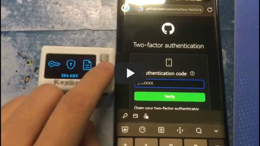
cannot be played, please click here to use BiliBili
Features

✅ Supports importing website keys from browser
✅ Supports TOTP 2FA real-time verification code binding
✅ Supports Bluetooth simulated input HID
✅ Supports WIFI NTP time synchronization
✅ Supports setting 6-digit device password
✅ Supports screen off
✅ Supports screen brightness adjustment. Plans

[ ] Access IoT Internet of Things Client
[ ] Weather, time, news, battery display

Open Source License
This project follows the CC BY-NC-SA 4.0 open source license. When using this program, please indicate the source and make a copyright statement.
This project is for learning and research purposes only. Unauthorized commercial profit is strictly prohibited.
If you have better suggestions, PR is welcome.
If you encounter any problems, please raise issues.
If you like this project, please give me a Star ⭐
Star History ChartReal picture


1
2


d83726536861c73bab3f8e9bc06b336bb1c62e45152e4ef3c35a244380875b

d71121f7d8fb372332b5ff2c4085806afcc41d5f515fb041ca14036da62cfe


PDF_KeyBox-ESP32C3.zip
Altium_KeyBox-ESP32C3.zip
PADS_KeyBox-ESP32C3.zip
BOM_KeyBox-ESP32C3.xlsx
92096
Desktop Weather Station Based on LCSC ESP32S3R8N8 Development Board
System Introduction:
This project is a desktop weather station based on the LCSC ESP32S3R8N8 development board. I have several ESP32 development boards, but I dare say that the LCSC ESP32S3R8N8 is the most aesthetically pleasing and fastest, bar none. This desktop weather station project includes functions such as real-time time acquisition, online weather forecast acquisition, local air pressure, temperature, and humidity acquisition, colored LEDs, and button functions.
PCB Design
Notes: The schematic diagram shows two screen interface designs: a 0.5mm pitch for plug-in connection and a 0.8mm pitch for soldering. The FPC adapter board is for extending the 0.8mm screen.
Software Description
Note: Partial Software Code
Blocks:
// 1. RGBLED Control
#include

// Initialize LED control instance
Adafruit_NeoPixel pixels(4, 11, NEO_GRB + NEO_KHZ800);

int16_t idx = 0; // Current LED pointer
unsigned int bright = 0; // Define brightness variable

// Light up RGBLED task
void TaskRgbLed(void *parameter)
{
while(1)
{
esp_random();
pixels.setPixelColor(0,pixels.Color(random(255),random(255),random(255)));
pixels.setPixelColor(1,pixels.Color(random(255),random(255),random(255)));
pixels.setPixelColor(2,pixels.Color(random(255),random(255),random(255)));
pixels.setPixelColor(3, pixels.Color(random(255), random(255), random(255)));

// bright++;
// bright%=256;
bright=20;
pixels.setBrightness(bright);
delay(1000);//delay, change speed
pixels.show(); // display
}
}

xTaskCreate(
TaskRgbLed,
"TaskRgbLed", // Task name
10000, // Size of the task stack, used to store the context information of the task runtime. Simply put, it can store up to this much information
NULL, /* Parameter passed as input of the task */
1, // Task priority, with 1 (configMAX_PRIORITIES - 1) is the highest, 0 is the lowest.
NULL); /* Task handle. */
// 2、I2C read pressure value
#include "Wire.h"
#define I2C_SDA 15
#define I2C_SCL 16
#define I2C_DEV_ADDR 0x60
float P=0.00; // Pressure
float T=0.00; // Temperature

// Read air pressure value
void getCps121(){
float buff[5]={0}; // Save the original temperature and pressure data: the first three digits are pressure, the last two digits are temperature
uint8_t bytesReceived=0;

Serial.println("Measuring atmospheric pressure and temperature");

// Send test command MR, wake up the device and perform a measurement
Wire.beginTransmission(0x6C);
Wire.write(0x30);
Wire.write(0xA);
Wire.endTransmission(true);

delay(100);

// Send read command, read data
Wire.beginTransmission(0x6C);
Wire.write(0x06);
Wire.endTransmission(true);
bytesReceived=Wire.requestFrom(0x6C,5,true);
if(bytesReceived==5)
{
buff[0] = Wire.read(); // Read the first data, pressure
buff[1] = Wire.read(); // Read the second data, pressure
buff[2] = Wire.read(); // Read the third data, pressure buff[3] = Wire.read(); // Read the fourth data, temperature
buff[4] = Wire.read(); // Read the fifth data, temperature
buff[4] = Wire.read(); // Read the fifth data, temperature buff[5] = Wire.read();

Serial.println(buff[0]);
Serial.println(buff[1])
;
Serial.println(buff[2]); Serial.println
(buff[3]);

x 256 + Pressure1st Byte [7:0]) / 2^6/1000
P = ((buff[0]*65536+buff[1]*256 + buff[2])/64)/1000;
Serial.printf("Pressure= %.2f kPa
",P);

//Positive Temperature [°C] = (Temperature High Byte [15:8] x 256 + Temperature Low Byte [7:0]) / 2^8 Negative Temperature [°C] = (Temperature High Byte [15:8] x 256 + Temperature Low Byte [7:0]-65536) / 2^8
T = (buff[3]*256 + buff[4])/256;
Serial.printf("Temperature= %.2f ℃
",T);
}
}
// 3, Light up the WorkLed task
void TaskWorkLed(void *parameter)
{
while(1)
{
// Set pin 48 to output low level
digitalWrite(48,LOW);
digitalWrite(10,LOW);
//digitalWrite(9,LOW);
// Delay 100ms
delay(500);
// Set pin 48 to output high level
digitalWrite(48,HIGH);
digitalWrite(10,HIGH);
//digitalWrite(9,HIGH);
// Delay 100ms
delay(500);

// The screen refresh is placed in the same thread, otherwise it will crash.
// Refresh time
digitalClockDisplay();

delay(100);

// Refresh weather
drawWeather();
}
//vTaskDelete(NULL);
}
4. Screen part
#include
#include
#include
#include
#include

// Screen pin definition
#define TFT_CS 48
#define TFT_RST 21
#define TFT_DC 40
#define TFT_MOSI 39 // SDA
#define TFT_SCLK 38 // SCL

// Create TFT object
Adafruit_ST7735 tft = Adafruit_ST7735(TFT_CS, TFT_DC, TFT_MOSI, TFT_SCLK, TFT_RST);
// Adafruit_ST7789 tft = Adafruit_ST7789(TFT_CS, TFT_DC, TFT_MOSI, TFT_SCLK, TFT_RST);

U8G2_FOR_ADAFRUIT_GFX u8g2; // Set font, support Chinese

// Screen theme, color
int Theme=1;
int backColor = BACK_WHITE; // BACK_BLACK;
uint16_t backFillColor = 0x0000;
int penColor = 0x0000;

// Initialize tft
void tftInit(){
tft.initR(INITR_BLACKTAB); // Initialize ST7735S 128x60
// tft.init(240, 320); // Initialize ST7789 320x240
tft.invertDisplay(false); // Disable invert color function
tft.setSPISpeed(40000000); // Set SPI_DEFAULT_FREQ
tft.setRotation(1); // Rotate display orientation 0,1

// Set theme color
if(Theme == 1){ // Originally a black theme, changed to white.
backColor = WHITE;
backFillColor = 0xFFFF;
penColor = 0x0000;
}else{
backColor = BLACK;
backFillColor = 0x0000;
penColor = 0xFFFF;
}

tft.fillScreen(backColor);// Set the screen background color
u8g2.begin(tft); // Establish a connection between u8g2 and Adafruit_ST77xx, very important, omitting this will cause an error
}

// Refresh the entire screen by background color
void reflashTFT(){
tft.fillScreen(backColor);
}

// Invert the screen color
void invertDisplayTFT(){
tft.invertDisplay(true);
delay(500);
tft.invertDisplay(false);
delay(500);
}

// Display text at a specified position
void drawtext(uint16_t x,uint16_t y,String text, uint16_t color) {
// 1. Use u8g2 for output, supporting Chinese characters
u8g2.setFont(FONT); // The Chinese font u8g2_font_wqy12_t_gb2312 has many fonts (around 210,000) while u8g2_font_wqy14_t_chinese1 has fewer fonts (around 14,000).
`u8g2.setFontMode(0); // Use u8g2's transparent mode (default)`
`u8g2.setFontDirection(0)
;` `u8g2.setForegroundColor(color); // Foreground color`
`u8g2.setBackgroundColor(WHITE); // Background color`
`u8g2.setCursor(x, y); // Text position`
`u8g2.print(text);
` }

// Draw the icon on the screen `
void drawicon()
{`
`u8g2.setFont(u8g2_font_siji_t_6x10); // Icon font`
`u8g2.setFontMode(1); // Use u8g2's transparent mode (default)`
`u8g2.setForegroundColor(BLACK);` Foreground color:
`u8g2.setBackgroundColor(WHITE);` // Background color
: `u8g2.drawGlyph(5, 12, 0x0e1ff);` // Power icon: `
u8g2.drawGlyph(160-16-5, 12, 0x0e21a);` // WiFi icon:

`u8g2.drawGlyph(10, 90, 0x0e015);` // Time icon:
`u8g2.drawGlyph(10, 40, 0x0e0cc);` // Temperature icon:
`u8g2.drawGlyph(10, 55, 0x0e0cf);` // Humidity icon: `
u8g2.drawGlyph(80, 40, 0x0e022);` // Weather icon: `u8g2.drawGlyph(80, 55, 0x0e083);` // Wind icon: `
u8g2.drawGlyph(80, 55, 0x0e083); ` // Draw the title void drawTitle(){ drawtext(35, 11, "ESP32 Desktop Weather Station", BLACK); } // Draw a rectangle void drawRectsBackground(uint16_t x,uint16_t y,uint16_t width,uint16_t height,uint16_t color) { //tft.fillScreen(WHITE); tft.drawRect(x, y,width,height, color); } // Draw a rounded rectangle void drawRoundRectsBackground(uint16_t x,uint16_t y,uint16_t width,uint16_t height,int16_t radius,uint16_t color) { //tft.fillScreen(WHITE); tft.drawRoundRect(x, y,width,height,radius,color); } // Draw a line void drawLine(uint16_t x1, uint16_t y1, uint16_t x2, uint16_t y2, uint16_t color) { tft.drawLine(x1, y1, x2, y2, color); } Important Notes for Physical Display : If you are a beginner like me, when purchasing a screen, be sure to specify "plug-in" in the notes. Do not solder it. Otherwise, you will regret it when you solder a broken screen. Don't ask me how I know; it's all tears.


If you accidentally bought a soldered one, it's best to make an FPC adapter cable. The seller sent me a soldered one, 18 pins, 0.8mm pitch. There weren't any ready-made FPC adapter cables for this pitch, so I had to design one myself. I used JLCPCB's FPC board for PCB fabrication, and after receiving it, I felt it was really good.
PDF_Desktop Weather Station Based on LCSC ESP32S3R8N8 Development Board.zip
Altium Desktop Weather Station Based on LCSC ESP32S3R8N8 Development Board.zip
PADS Desktop Weather Station Based on LCSC ESP32S3R8N8 Development Board.zip
BOM_Desktop Weather Station Based on LCSC ESP32S3R8N8 Development Board.xlsx
92097
electronic
参考设计图片
×
 
 
Search Datasheet?

Supported by EEWorld Datasheet

Forum More
Update:2026-03-28 00:31:03
  • 2022 Digi-Key Innovation Design Competition Unboxing
  • Switching Circuit
  • To learn the best skills
  • A classic book introducing DSP external circuit design
  • WinCE 5.0 USB Mass Storage question
  • University Electronic Design Temperature PWM

EEWorld
subscription
account

EEWorld
service
account

Automotive
development
community

Robot
development
community

About Us Customer Service Contact Information Datasheet Sitemap LatestNews


Room 1530, 15th Floor, Building B, No.18 Zhongguancun Street, Haidian District, Beijing, Postal Code: 100190 China Telephone: 008610 8235 0740

Copyright © 2005-2024 EEWORLD.com.cn, Inc. All rights reserved 京ICP证060456号 京ICP备10001474号-1 电信业务审批[2006]字第258号函 京公网安备 11010802033920号