Listed below are the reference design's key specifications, detailed schematic ( Figure 1 ), and bill of materials ( Table 1 ).
Design specifications and configurations
Wide input voltage range of 2.7V to 11V
70V output voltage
4mA output current
400kHz fixed switching frequency
-40°C to +125°C operating temperature range
Miniature, 8mm x 12mm board size
Figure 1 shows the schematic of the reference design with an input voltage range of 2.7V to 5.5V. By connecting the CP pin to V IN and removing the charge pump capacitor (C3), the circuit accepts a 5.5V to 11V input range.
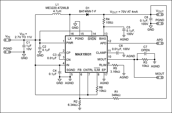
Figure 1. MAX15031 boost converter schematic, F SW = 400kHz (fixed).
All reference designs on this site are sourced from major semiconductor manufacturers or collected online for learning and research. The copyright belongs to the semiconductor manufacturer or the original author. If you believe that the reference design of this site infringes upon your relevant rights and interests, please send us a rights notice. As a neutral platform service provider, we will take measures to delete the relevant content in accordance with relevant laws after receiving the relevant notice from the rights holder. Please send relevant notifications to email: bbs_service@eeworld.com.cn.
It is your responsibility to test the circuit yourself and determine its suitability for you. EEWorld will not be liable for direct, indirect, special, incidental, consequential or punitive damages arising from any cause or anything connected to any reference design used.
Supported by EEWorld Datasheet
EEWorld
subscription
account

EEWorld
service
account

Automotive
development
community

Robot
development
community

About Us Customer Service Contact Information Datasheet Sitemap LatestNews


Room 1530, 15th Floor, Building B,
No.18 Zhongguancun Street,
Haidian District,
Beijing, Postal Code: 100190
China
Telephone: 008610 8235 0740
 京公网安备 11010802033920号

 7404
7404


