The maximum input power of the POE power supply depends on the power classification of the powered device (PD). For level 0 PD, the maximum power is 12.95W; for level 1 PD, the power is 3.85W. This application note describes a three-output, 3.12W, high-efficiency POE power supply with ±5% stable output.
Key Features of Power Supplies
275kHz switching frequency
Comply with IEEE802.3af power supply standard
Integrates an IEEE802.3af compliant POE interface and PWM controller in a 16-pin SO package ( MAX5941A )
flyback topology
Synchronous rectification output
Isolated output with AC isolation voltage up to 1500V
All outputs are stable within ±5%
Output: +3.3V (0.2A), +2.5V (0.6A) and +1.2V (0.8A)
The circuit in Figure 1 is a three-output POE power supply composed of a POE interface that complies with the IEEE802.3af standard and a PWM current mode controller (U2) MAX5941A. The 3.3V and 2.5V outputs of the power supply use a synchronous rectification flyback topology, and the 1.2V output is generated from 3.3V by a synchronous rectification buck converter. The circuit schematic does not include the diode rectifier bridge in the input section.
Half of the MAX5941A IC is used to generate the POE interface. The DC output of the diode rectifier bridge is added to both ends of capacitor C10. Zener diode D4 protects the MAX5941A from overvoltage. The MAX5941A's internal hot-swap MOSFET turns on at 39V and slowly charges C6 to 40V. The conduction of the MOSFET limits the inrush current. When C6 is almost charged to the input voltage, the PGOOD signal goes high. R10 is the PD detection resistor, and R25 is the classification resistor.
The other half of the circuit of MAX5941A is the PWM control part. When power is applied to the PWM part, the PWM controller starts working. Soft-start capacitor C14 slowly increases the primary peak current of the power transformer.
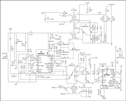
Figure 1. Schematic of the power supply ( Download PDF )
All reference designs on this site are sourced from major semiconductor manufacturers or collected online for learning and research. The copyright belongs to the semiconductor manufacturer or the original author. If you believe that the reference design of this site infringes upon your relevant rights and interests, please send us a rights notice. As a neutral platform service provider, we will take measures to delete the relevant content in accordance with relevant laws after receiving the relevant notice from the rights holder. Please send relevant notifications to email: bbs_service@eeworld.com.cn.
It is your responsibility to test the circuit yourself and determine its suitability for you. EEWorld will not be liable for direct, indirect, special, incidental, consequential or punitive damages arising from any cause or anything connected to any reference design used.
Supported by EEWorld Datasheet
EEWorld
subscription
account

EEWorld
service
account

Automotive
development
community

Robot
development
community

About Us Customer Service Contact Information Datasheet Sitemap LatestNews


Room 1530, 15th Floor, Building B,
No.18 Zhongguancun Street,
Haidian District,
Beijing, Postal Code: 100190
China
Telephone: 008610 8235 0740
 京公网安备 11010802033920号

 7511A87-450


