The AD5933 and AD5934 are high-precision impedance converter system solutions that combine an on-chip programmable frequency generator with a 12-bit, 1 MSPS (AD5933) or 250 kSPS (AD5934) analog-to-digital converter (ADC). An adjustable frequency generator generates a known frequency to excite an external complex impedance.
The circuit shown in Figure 1 produces accurate impedance measurements in the low ohm range up to hundreds of kΩ while also optimizing the overall accuracy of the AD5933/AD5934.

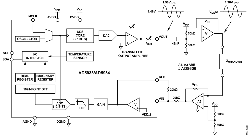
The AD5933 and AD5934 offer four programmable output voltage ranges, each with an associated output impedance. For example, the output impedance for a 1.98V pp output voltage is typically 200 Ω (see Table 1).
| Range | Output Excitation Amplitude | Output Resistance, ROUT |
| Range 1 | 1.98V pp | 200Ωtyp |
| Range 2 | 0.97Vpp | 2.4 kΩ type |
| Range 3 | 0.383Vpp | 1.0 kΩ type |
| Range 4 | 0.198Vpp | 600Ωtyp |
This output impedance affects measurement accuracy, especially in the low kΩ range, so it should be taken into account when calculating the gain coefficient. See the AD5933 or AD5934 data sheet for details on gain factor calculations. A simple buffer within the signal chain prevents the output impedance from affecting unknown impedance measurements. When selecting a low output impedance amplifier, sufficient bandwidth should be ensured to adapt to the excitation frequency of the AD5933/AD5934. For the AD8605 / AD8606 / AD8608 series CMOS operational amplifiers, an implementation example of low output impedance is shown in Figure 2. The output impedance of this amplifier is less than 1 Ω (up to 100 kHz) at AV=1, which is the maximum operating range of the AD5933/AD5934.


DC offset matching of transmitter and receiver stages
The four programmable output voltage ranges of the AD5933/AD5934 have four associated bias voltages (Table 2). For example, a 1.98 V pp excitation voltage is biased at 1.48 V. However, as shown in Figure 1, the current-to-voltage (IV) receiver stage of the AD5933/AD5934 is set to a fixed bias of VDD/2. Therefore, for a 3.3V supply, the transmit bias is 1.48 V, while the receive bias is 3.3 V/2 = 1.65 V. This potential difference causes impedance polarization during testing and can lead to inaccurate impedance measurements.
One solution is to add a simple high-pass filter with a corner frequency in the low Hz range. Removes the DC bias from the transmitter stage and re-biases the AC signal to VDD/2, keeping the DC level constant throughout the signal chain.
| Range | Output Excitation Amplitude | Output DC Bias Level |
| 1 | 1.98V pp | 1.48V |
| 2 | 0.97Vpp | 0.76V |
| 3 | 0.383Vpp | 0.31V |
| 4 | 0.198Vpp | 0.173V |
Select an IV buffer optimized for the receive stage
The current-to-voltage (IV) amplifier stage of the AD5933/AD5934 may also slightly add to the inaccuracy of the signal chain. The IV conversion stage is susceptible to the amplifier's bias current, offset voltage, and CMRR. By selecting an appropriate external discrete amplifier to perform the IV conversion, the user can select an amplifier with low bias current and offset voltage specifications and excellent CMRR to improve the accuracy of the IV conversion. This internal amplifier can then be configured as a simple inverting gain stage.
As stated in the AD5933/AD5934 data sheet, the resistor R FB is still selected based on the overall gain of the system.
Optimized signal chain for high-precision impedance measurements
Figure 1 shows a recommended configuration for measuring low-impedance sensors. The AC signal is high-pass filtered and re-biased before being buffered using an ultra-low output impedance amplifier. After the IV conversion is completed externally, the signal is returned to the AD5933/AD5934 receiving stage. The key specifications that determine the required buffer are ultra-low output impedance, single-supply capability, low bias current, low offset voltage, and excellent CMMR performance. Some recommended devices include the ADA4528-1 , AD8628 / AD8629 , AD8605 and AD8606. Depending on the board layout, a single or dual channel amplifier can be used. Both the bias resistor (50kΩ) and the gain resistor (20kΩ and R FB ) use 0.1% accuracy resistors to reduce inaccuracy.


Blockdiagram
All reference designs on this site are sourced from major semiconductor manufacturers or collected online for learning and research. The copyright belongs to the semiconductor manufacturer or the original author. If you believe that the reference design of this site infringes upon your relevant rights and interests, please send us a rights notice. As a neutral platform service provider, we will take measures to delete the relevant content in accordance with relevant laws after receiving the relevant notice from the rights holder. Please send relevant notifications to email: bbs_service@eeworld.com.cn.
It is your responsibility to test the circuit yourself and determine its suitability for you. EEWorld will not be liable for direct, indirect, special, incidental, consequential or punitive damages arising from any cause or anything connected to any reference design used.
Supported by EEWorld Datasheet
EEWorld
subscription
account

EEWorld
service
account

Automotive
development
community

Robot
development
community

About Us Customer Service Contact Information Datasheet Sitemap LatestNews


Room 1530, 15th Floor, Building B,
No.18 Zhongguancun Street,
Haidian District,
Beijing, Postal Code: 100190
China
Telephone: 008610 8235 0740
 京公网安备 11010802033920号

 177-714-1-100GP8K5-24MAN


