This project mainly utilizes the GD32E230C8T6 minimum system board, analog front-end processing circuit, comparator frequency measurement circuit, PWM output circuit, and TFT screen driving circuit to construct a simple digital oscilloscope for detecting various signal outputs in actual circuits.
I. Functional Implementation Ideas
The core of this project is to use the ADC detection function of the GD32E230C8T6 minimum system board to display the detected ADC value as a curve on the TFT screen. Through the operation of the interactive circuit, the displayed waveform and the output PWM signal are controlled. It can be mainly divided into six parts: power supply, measured signal input, microcontroller processing, control signal input, display and indication, and PWM output. The connections between these parts are detailed in Figure 1. Figure

1: Simple Oscilloscope Functional Implementation Figure
1.1 Power Supply Section
The power supply section mainly consists of a Type-C power input circuit (input +5V) and a negative voltage generation circuit (generate -5V). Its main function is to provide power (+5V and -5V) for the entire project. See the schematic diagram for details.
1.2 Test Signal Input Section
The test signal input section is mainly divided into an analog front-end signal input acquisition circuit and a comparison frequency measurement circuit. The main function of the analog front-end signal input acquisition circuit is to process the test signal to obtain the ADC; the main function of the comparison frequency measurement circuit is to process the ADC to obtain the input frequency signal.
1.3 Microcontroller Processing Section
The microcontroller processing section is mainly the GD32E230C8T6 minimum system board, which is the brain of the entire project. It is responsible for signal acquisition, communication with the TFT after acquiring the signal from the interactive circuit, control of the indicator circuit for display, PWM output, etc.
1.4 Control Signal Input Section
The control signal input section is mainly the interactive circuit. Its main function is for the operator to generate level signals through knobs and buttons. The GD32E230C8T6 minimum system board acquires these high and low levels and performs display changes or other operations (by program design).
1.5 Display and Indication Section
The display and indication section mainly consists of a TFT display screen and LED indicator circuits. Its main function is to display waveforms and perform display changes or other operations after the GD32E230C8T6 minimum system board obtains the high and low levels of the control input (programmed).
1.6 PWM Output Section The
PWM output section mainly consists of a PWM output circuit. Its main function is to output PWM signals using the GD32E230C8T6 minimum system board (programmed).
II. Schematic Design
Based on the functional implementation approach, the schematic design mainly includes a Type-C power input circuit, a negative voltage generation circuit, an analog front-end signal input acquisition circuit, a comparator frequency measurement circuit, the GD32E230C8T6 minimum system board, a five-way switch circuit, a button control circuit, a 1.8-inch TFT interface driver circuit, an LED indicator circuit, and a PWM interface circuit—a total of 10 subdivided circuits. See the appendix for the complete circuit diagram.
The GD32E230C8T6 minimum system board, five-way switch circuit, button control circuit, 1.8-inch TFT interface driver circuit, LED indicator circuit, and PWM interface circuit are relatively simple; please refer to the attached schematic diagram for wiring details. The following is a simple analysis of the Type-C power input circuit, negative voltage generation circuit, analog front-end signal input acquisition circuit, and comparator frequency measurement circuit:
2.1 Type-C Power Input Circuit
Based on the functional implementation, the Type-C power input circuit mainly provides a +5V power supply voltage to the oscilloscope. It can be directly powered through an external Type-C port. The oscilloscope is turned on/off via a slide switch, and an LED display is added to indicate whether the power supply is normal (see Figure 2). R1 is for current limiting to prevent LED1 from burning out; C1 is for power filtering.

Figure 2 Type-C Power Input Circuit
2.2 Negative Voltage Generation Circuit
Following the functional implementation approach, the negative voltage generation circuit mainly provides a -5V power supply voltage to the oscilloscope. This can be directly implemented using the XD7660 chip. Basically, the design follows the XD7660 datasheet; see Figure 3 for details.

Figure 3 Negative Voltage Generation Circuit
2.3 Analog Front-End Signal Input Acquisition Circuit
Following the functional implementation approach, the analog front-end signal input acquisition circuit mainly processes the input signal, including four stages: coupling method, attenuation setting, voltage follower, and proportional amplification, to obtain the acquired ADC; see Figure 4 for details.

Figure 4 Analog Front-End Signal Input Acquisition Circuit
2.3.1 Coupling Mode Control
The coupling mode is divided into DC coupling and AC coupling. After the signal under test is input from RF1, it is selected by sliding switch SW2. When contact 2 of SW2 is in contact with contact 1, the DC signal is directly coupled to the next stage circuit, and the AC signal is connected to ground through C6. At this time, the coupling mode is DC coupling (see the light green signal in Figure 4). When contact 2 of SW2 is in contact with contact 3, due to the characteristic of capacitor C5 that passes AC and blocks DC, only the AC signal is coupled to the next stage circuit. At this time, the coupling mode is AC coupling (see the light yellow signal in Figure 4).
2.3.1 The attenuation setting
can be set to direct input or 1/50 attenuation. After the signal under test is input from RF1, it is selected via the sliding switch SW2. When contact 2 of SW2 is in contact with contact 1, the DC signal is directly coupled to the next stage circuit, and the AC signal is connected to ground through C6. At this time, the coupling method is DC coupling (see the bright green signal in Figure 4). When contact 2 of SW2 is in contact with contact 3, due to the AC-passing and DC-blocking characteristic of capacitor C5, only the AC signal is coupled to the next stage circuit. At this time, the coupling method is AC coupling (see the yellow signal in Figure 4). The attenuation ratio is 1/50. The calculation process is shown in the dark yellow part of Figure 4.
2.3.1 Voltage Follower
The voltage follower mainly utilizes the virtual short and virtual open characteristics of the operational amplifier TL072I to prevent excessive input current from burning out the circuit.
2.3.3 Proportional Amplification The proportional amplifier
mainly uses the operational amplifier TL072I and its peripheral circuits to adjust the input voltage amplitude to achieve a wider range of voltage acquisition. The proportional amplifier circuit analysis is shown in the dark yellow part of Figure 4.
2.4 Comparator Frequency Measurement Circuit
Following the functional implementation approach, the comparator frequency measurement circuit still processes the acquired signal to obtain its frequency. The high and low levels at the output terminal can be used to deduce the input threshold of the ADC in the comparator circuit; adjusting the resistor values in the comparator circuit can adjust the ADC input threshold; the GD32E230C8T6 obtains the frequency of the input signal by detecting the time interval between the high and low levels of the input.

Figure 5 Comparator Frequency Measurement Circuit
III. PCB Design
PCB design varies from person to person, based on personal preferences and design habits. Here, to save space, the BNC interface and the GD32E230C8T6 system board are placed on the bottom layer, as shown in Figures 6, 7, and 8.

Figure 6 Simple Oscilloscope PCB (Top)

Figure 7 Simple Oscilloscope PCB (Bottom)

Figure 8. Simple Oscilloscope PCB 3D Simulation Diagram.
IV. PCB Prototyping and Soldering.
After the PCB design is completed, you can place an order for prototyping. While waiting, purchase the necessary components. See the attachment for the BOM. Once everything is in place, you can start soldering. See Figures 9, 10, and 11 for photos of the soldered product.

Figure 9. Simple Oscilloscope Product (After Soldering)

Figure 10. Simple Oscilloscope Product (With TFT Screen - Front)

Figure 11. Simple Oscilloscope Product (Back)
V. Housing Design and 3D Printing.
You can export the simple oscilloscope PCB 3D simulation model as STEP format and then import it into 3D modeling software such as SolidWorks or Shapr 3D. Then, model the housing. See Figure 12 for details.

Figure 12. Simple Oscilloscope Housing Design (Front).
After modeling, export the STL file and then place an order for 3D printing (those with a 3D printer can print it themselves).
VI. Program Verification.
The program can be found in the attachments. Figure 13 shows the burning verification, Figure 14 shows

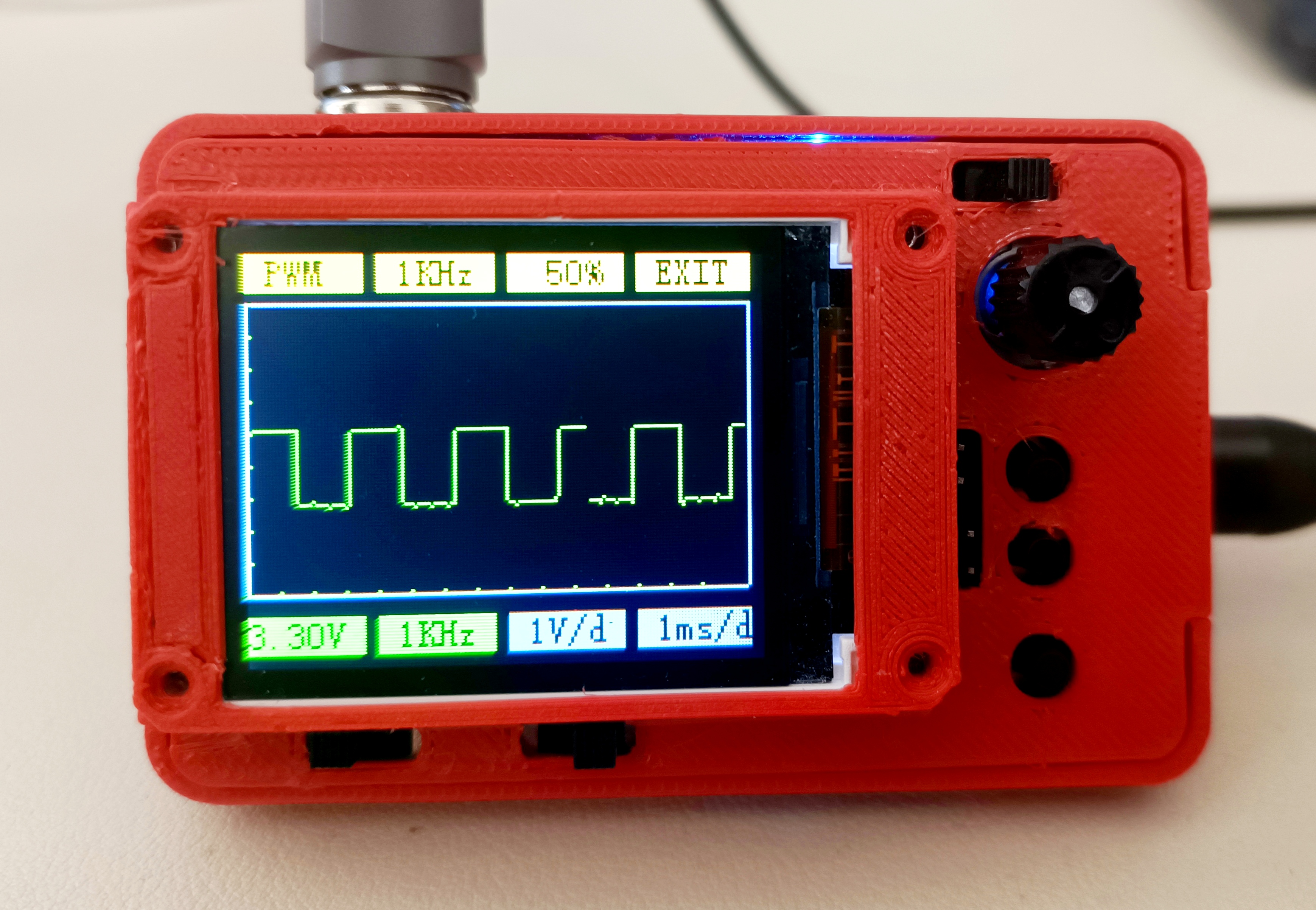
the burning software interface, and Figure 14 shows the interface after burning the program. VII. Summary First, I'd like to thank LCSC for this event. I learned how to operate the GD32E230C8T6 microcontroller and also received this simple oscilloscope prototype. Secondly, I encountered some minor issues during the process, mainly twofold: firstly, after replacing the through-hole components with surface-mount components, several polarized capacitors were not easy to solder (the pads were too small); secondly, due to the screen orientation, the program content needed adjustment. Otherwise, everything went relatively smoothly, and the overall difficulty was not high. Those interested can also try to replicate it. Finally, regarding the finished product, the final product is quite compact, about the size of a palm. Unfortunately, I couldn't use LCSC's 3D printing voucher (it expired before I could activate it, lol), so I had to print it myself. Figure 15 shows the size comparison . Finally, I've attached a picture of the adjusted interface, which feels simpler. More modes can be developed in the future. Figure 16 UI Reconstruction ------------------------------------------------------------------------------------------ Divider ------------------------------------------------------------------------------------ The button functions have been reconstructed in the new interface, adding grid adjustment, Ua-Ub, ta-tb, and displacement functions. The implementation logic of the button functions is shown in Figure 17. Adjustments were made based on the code example provided by LCSC. For a detailed demonstration of the functions, please see attached video 2. The hex file (Oscilloscope - newUI.hex) is also attached; you can download and burn it if you want to try it. Figure 17 Reconstructing Button Functions This project is currently considered complete. Further optimization will be done later when time permits.


 京公网安备 11010802033920号

 MSP1N5267ATR


