
In introduction,
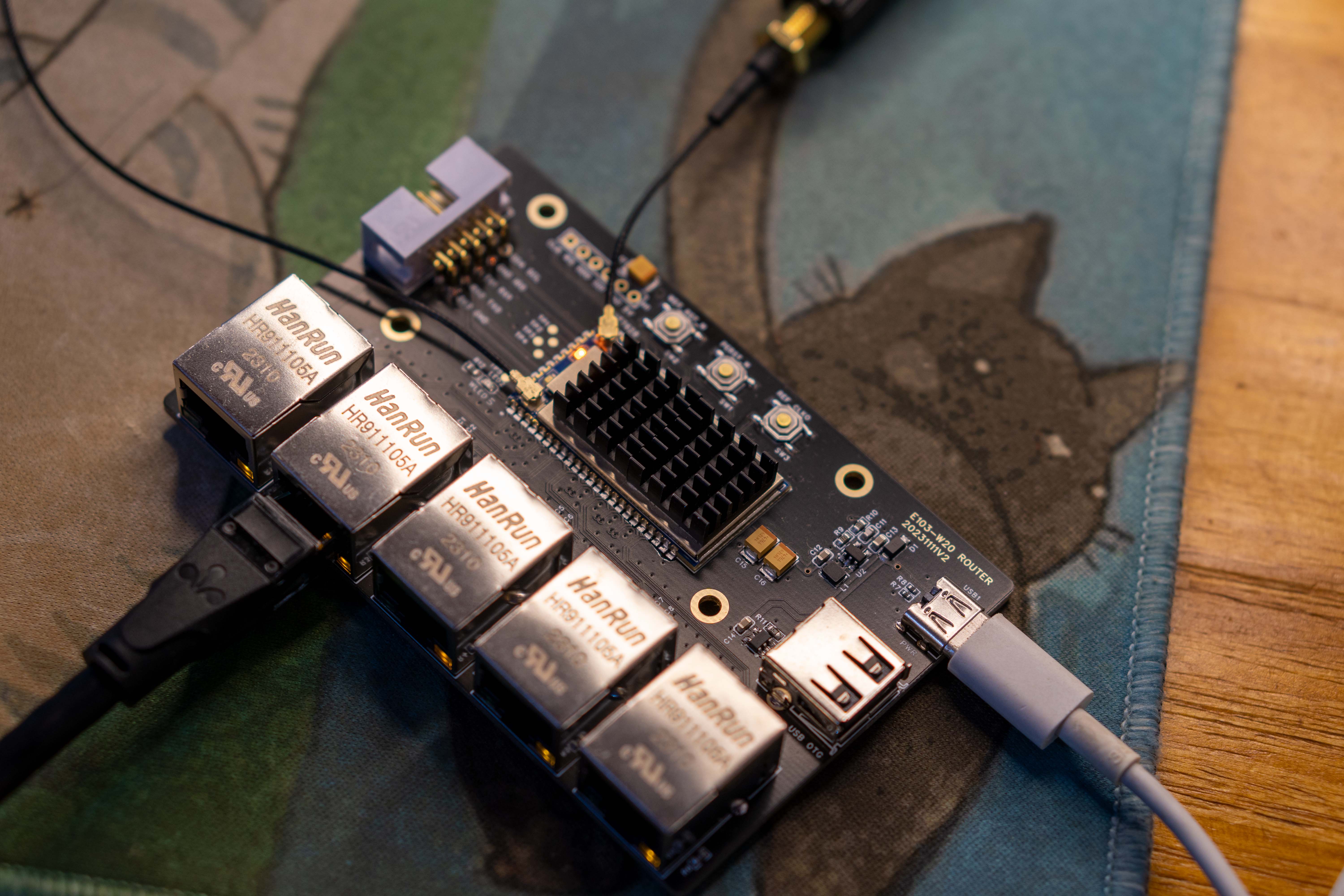
this project, based on the EBITA E103-W20 MT7628 module, implements an ultra-low-cost router. The MT7628 is a high-performance router chip with a long history and abundant documentation. It can be used as an introductory chip for learning OpenWRT, or as an IoT gateway to enable device-to-cloud connectivity.
Reference Project
: Thanks to the project of the expert: https://oshwhub.com/toolchen/mini-router
Update Log:
2023-11-19 First Release
2023-11-22 Added 5.10 kernel firmware, enhanced WIFI stability, recommended update.
Basic Features:
Five 10M/100M Ethernet ports, internal integrated switch (one defaults to WAN port, four defaults to WAN port),
2.4G Wifi, 2T2R
580MHz MIPS core processor,
USB 5V power supply
, USB 2.0 interface, can be used for external network port or USB storage,
32MB Flash,
128M DDR2 RAM
, two TTL serial ports, one for Linux log printing,
one I2C interface.
Chip
Solution: Main Chip Module: E103-W20 MT7628 module,
SY8089A1AAC 5V TO 3V3 DCDC
, SY6280 USB 2A current limiting protection chip,
HR911105A. This document describes the flashing of MTK Breed firmware using the built-in network adapter and
OpenWRT firmware. Since the module's built-in U-Boot is difficult to use and lacks progress tracking, we opted for the U-Boot developed by a skilled flashing developer. Before flashing, you need to enter the built-in U-Boot. The flashing process is as follows: First, connect the device's LAN port to the network cable and the other end to the computer, ensuring a stable connection. Then, modify the network port address to match the U-Boot update address (see image below). After setting this up, press and hold the PERST_N button, connect the device to USB power, and wait a few seconds until U-Boot boots. Open a browser and access 192.168.1.111. Normally, you should see the built-in U -Boot update interface. As shown in the image above, select the Breed firmware (breed-mt7688-reset38.bin is provided in the attachment), and then click "Update U-Boot." Wait for the update to complete, as shown in the image below. After flashing, the system will automatically restart. Since there is no progress display, it is recommended to wait a few more seconds to prevent corrupting U-Boot! After entering the Unbreakable Uboot interface and modifying the options, wait for the flashing process to complete. Then, disconnect the board's power, change the network port IP address to automatic acquisition, and press and hold the PERST_N button (the same button as before) while connecting the board to the power supply. If Uboot boots successfully, the network port LED will flash a few times, and an Ethernet IP address will be assigned. Enter 192.168.1.1 in your browser to access the Unbreakable Uboot interface. The interface parameters should display correctly (optional). Click "Firmware Backup" to back up the current system partition (the system partition contains the original EEPROM, which is not accessible to ordinary users; it is only available during manufacturer development and flashed at the factory). If the firmware is corrupted later, a programmer will be needed to recover the bricked board. Click "Firmware Update" to flash the new OpenWRT firmware, as shown in the image (the test firmware in the attachment can be used). The update process is shown in the image below. After the update is complete, the system will automatically restart. If using the test firmware, the system will be able to find a Wi-Fi hotspot named "OpenWRT" after startup. Connect to it and enter the password to access the background test firmware. The firmware is based on the latest LEDE source code and includes basic plugins and Flow Offloading to improve forwarding efficiency, making it suitable for basic use. Setting up the basic development environment for OpenWRT firmware : This article will use WSL (Windows Subsystem for Linux) to develop and compile OpenWRT firmware. WSL needs to be enabled first (refer to Baidu for details). After enabling it, download Ubuntu 20 from the app store. After downloading, start the system and complete the initial password and other configurations. Disabling Windows Path: Including this configuration in the Windows path will cause the source code compilation to fail. You need to disable it. Edit `/etc/wsl.conf` and add the following content: ` [interop] appendWindowsPath = false`. Then, enter `wsl --shutdown` in the Windows terminal to restart the WSL environment. After restarting, enter the following commands to install the basic compilation environment: `sudo apt update -y` `sudo apt full-upgrade -y` `sudo apt install -y` The output will include the following programs: `ack antlr3 asciidoc autoconf automake autopoint binutils bison build-essential bzip2 ccache cmake cpio curl device-tree-compiler fastjar flex gawk gettext gcc-multilib g++-multilib git gperf haveged help2man intltool libc6-dev-i386 libelf-dev libglib2.0-dev libgmp3-dev libltdl-dev libmpc-dev libmpfr-dev libncurses5-dev libncursesw5-dev libreadline-dev libssl-dev libtool lrzsz mkisofs msmtp nano ninja-build p7zip p7zip-full patch pkgconf python2.7 python3 python3-pyelftools libpython3-dev` Download the source code for qemu-utils, rsync, scons, squashfs-tools, subversion, swig, texinfo, uglifyjs, upx-ucl, unzip, vim, wget, xmlto, xxd, zlib1g-dev, and python3-setuptools.


Since the official OpenWRT MT7628 WIFI uses an open-source driver, it cannot unlock higher power. Also, the latest official version does not support the 5.4 kernel, which causes frequent WIFI disconnections. Therefore, we chose the lede source code from lean. This project is basically compatible with OpenWRT and can completely replace development.
Source code GitHub address: https://github.com/coolsnowwolf/lede
Enter the following commands to download the lede repository and the accompanying libraries, then enter the configuration interface:
git clone https://github.com/coolsnowwolf/ledecd lede ./scripts/feeds update -a ./scripts/feeds install -amake menuconfig
Select the target to develop
Refer to the image below

Luci plugin configuration
Luci is used to configure OpenWRT related information on the webpage. A series of plugins provided by lede are also provided in the form of webpages. We can enable the required plugins, as shown in the image below:

Applications enabled in the test firmware
luci-app-arpbind............................................. ARP Binding luci-app-autoreboot.................... LuCI support for Scheduled Reboot luci-app-filetransfer........................... LuCI page for IPK upload -*- luci-app-firewall................ Firewall and Portforwarding application luci-app-ttyd...................................... LuCI support for ttyd luci-app-turboacc............ LuCI support for Flow Offload / Shortcut-FE[*] Include Flow Offload[*] Include BBR CCA[*] Include Pdnsd luci-app-upnp................. Universal Plug & Play configuration module luci-app-vnstat.................................. LuCI Support for VnStat
Kernel module configuration
: Select Kernel modules on the first screen to enter the kernel module configuration interface.
USB storage device configuration:
Block Devices --->
-*- kmod-scsi-core....................................... SCSI device support
Filesystems --->
kmod-fs-ext4..................................... EXT4 filesystem support
kmod-fs-ntfs3.......... NTFS filesystem read & write (new driver) support
kmod-fs-vfat..................................... VFAT filesystem support
USB Support --->
kmod-usb2................................... Support for USB2 controllers
-*- kmod-usb-storage..................................... USB Storage support kmod-usb-storage-extras.................... Extra drivers for usb-storage kmod-usb-storage-uas.................... USB Attached SCSI (UASP) support
Enable USB network adapter
USB Support --->
-*- kmod-usb-net............... Kernel modules for USB-to-Ethernet convertors
kmod-usb-net-asix...... Kernel module for USB-to-Ethernet Asix convertors kmod-usb-net-asix-ax88179
kmod-usb-net-rndis......................... Support for RNDIS connections
OCHI
USB Support --->
kmod-usb-ohci............................... Support for OHCI controllers
Button
Input modules --->
kmod-input-gpio-keys.................................... GPIO key support
Configuration of related tools
Utilities --->
usbutils................................... USB devices listing utilities
Network --->
iperf3........................ Internet Protocol bandwidth measuring tool
Kernel version configuration
Downgrade kernel to 5.4
Edit `target/linux/ramips/Makefile`
and configure the following two options to 5.4, referring to the following content:
`KERNEL_PATCHVER:=5.4` `KERNEL_TESTING_PATCHVER:=5.4` For
device tree configuration
, we can configure IO mapping according to requirements based on the original configuration. The relevant nodes can be referenced in the `mt7628an.dtsi` file. We need to modify `mt7628an_hilink_hlk-7628n.dts` (it is recommended to use the file in the attachment), located in `lede argetlinux
amipsdts`. You can refer to the modified file below:
// SPDX-License-Identifier: GPL-2.0-or-later OR MIT
#include "mt7628an.dtsi"
#include
#include
/ {
compatible = "hilink,hlk-7628n", "mediatek,mt7628an-soc";
model = "HILINK HLK-7628N";
keys {
compatible = "gpio-keys";
reset {
label = "reset";
gpios = ;
linux,code = ;
};
};
leds {
compatible = "gpio-leds";
wlan {
label = "green:wlan";
gpios = ;
};
led1 {
label = "led1";
gpios = ;
};
led2 {
label = "led2";
gpios = ;
};
led3 {
label = &
i2c
{
status = "okay";
};
&i2s {
status = "okay";
};
&gdma {
status = "okay";
};
&uart1 {
status = "okay";
};
&spi0 {
status = "okay";
pinctrl-names = "default";
pinctrl-0 = , ;
flash@0 {
compatible = "jedec,spi-nor";
reg = ;
spi-max-frequency = ;
broken-flash-reset;
partitions {
compatible = "fixed-partitions";
#address-cells = ;
#size-cells = ;
partition@0 {
label = "u-boot";
reg = ;
read-only;
};
partition@30000 {
label = "u-boot-env";
reg = ;
read-only;
};
factory: partition@40000 {
label = "factory";
reg = ;
read-only;
};
partition@50000 {
compatible = "denx,uimage";
label = "firmware";
reg = ;
}; }
;
};
};
ðernet {
mtd-mac-address = ;
};
&wmac {
status = "okay";
};
To compile
, enter the following commands to start compiling:
make download -j8 make V=s -j16
The compiled files are stored in targets
amipsmt76x8, and the file ending with sysupgrade.bin is the file to be burned.
Showing pictures


breed-mt7688-reset38.bin
(20231109)openwrt-ramips-mt76x8-hilink_hlk-7628n-squashfs-sysupgrade.bin
mt7628an_hilink_hlk-7628n.dts
(20231122KERNEL510)openwrt-ramips-mt76x8-hilink_hlk-7628n-squashfs-sysupgrade.bin
PDF_MT7628 Ultra-Low Cost Router.zip
Altium_MT7628 Ultra-Low Cost Router.zip
PADS_MT7628 Ultra-Low Cost Router.zip
BOM_MT7628 Ultra-Low Cost Router.xlsx
91435
JMS578-based USB to SATA hard drive enclosure [Verified]
Type-C USB 3.2 Gen1 to SATA adapter based on JMS578+VL160
I. Main Controller
1. Overview
The JMS578 is a USB 3.2 Gen 1 to SATA 6Gb/s bridge controller, a low-power, high-performance solution for external solid-state drives, hard disk drives, and optical discs. Compared to previous products, the JMS578 offers higher data transfer rates and lower power consumption. Furthermore, the JMS578 is a data storage solution using a two-layer printed circuit board design, thus providing customers with a more cost-effective solution.
2. Key Features
: Complies with SATA 6Gb/s electrical specification version 3.2
; Complies with USB 3.0 specification, USB Mass Storage Class, BOT specification, and UASP specification
; Supports USB Ultra/High-Speed/Full-Speed operation
; Supports SHA-1/SHA-256 for IEEE-1667 digest calculation;
Supports external SPI NVRAM for Vendor VID/PID for USB 2.0/USB 3.0 device controllers;
Supports ATA/ATAPI PACKET command set;
Provides hardware-controlled PWM.
3. Block Diagram

II. Interface Definition
1. Relationship between Transmission Standards and Interface Support

2. Type-C 24-Pin:
Because USB 3.0 (USB 3.2 Gen1) data transmission is required, and considering that Type-C data cables are more commonly used, this interface is chosen.
The following diagram shows the pin functions and definitions of the 24-Pin Type-C male and female connectors.
It is clear that

the pin

functions within the connector are symmetrical about the center. The pin functions perfectly match when the male connector is inserted into the female connector, regardless of whether it is inserted in the correct orientation. Furthermore, both VBUS and GND power supplies have 4 pins, supporting a maximum current of 5A, which improves current carrying capacity while ensuring high-speed data transmission.
Pin Function Definitions

3. SATA
Interface Definition

Data Interface (7 pins) Definition

Power Interface (15 pins) Definition


III. Hardware Design Considerations
1. USB 3.0 Design Considerations
Impedance Control: It is recommended that the differential impedance of USB 3.0 be controlled at 90Ω with a tolerance of 10%, and the differential impedance of USB 2.0 be controlled at 90Ω with a tolerance of 10%.
Delay Control: It is recommended that the differential pairs of USB 3.0 be designed with equal lengths, with an error of less than 5mil. The equal length error control for USB 2.0 is less than 10mil.
DC Blocking Capacitor: It is recommended to select capacitors with packages below 0402, with a capacitance value between 75nF and 265nF as required by the official SPEC, and place them close to the terminals during layout.
Internal Crossover: If there is crossover on the USB 3.0 P/N traces, the P/N of the differential pair can be swapped. USB 3.0 allows P/N reversal. (Remember, this is only for USB 3.0; do not swap out the 2.0 version!)
2. SATA Design Considerations:
AC coupling capacitors with a value of 10nF (below 12nF) should be placed close to the connector. Place
AC coupling capacitors symmetrically; choose small package sizes, at least 0402.
Place all SATA transmit and receive coupling capacitors at the connector end to avoid reflections from the board to the device.
100Ω differential impedance design:
No equal length requirements for
transmit and receive. Cut out pads and vias. Add
two ground vias at layer changes. Keep differential signals away from crystal oscillators and high-speed clocks.
Ensure a complete ground reference to guarantee impedance continuity.
IV. Physical Testing:
Since I didn't have a suitable hard drive on hand, I used some unused drives from disassembled machines.
1. Seagate 500G mechanical hard drive (empty).


I said I had tools... but couldn't put it out...
2. Samsung SSD 256G (half-drive)


V. About Firmware
The firmware is attached. This working firmware was copied from an imported easy-drive cable. Due to firmware issues, I initially thought there was a problem with my previous double-layer board design, hence this rudimentary four-layer board version (meaning it doesn't use DC-DC converters or power management; direct connection is less prone to errors).
Testing showed the latest version 188.02.00.01 didn't work; the drive wasn't recognized upon power-on, even without the hard drive plugged in. An extra hard drive was still visible in Disk Management, as shown in the image below.


If the TX/RX of the SATA drive is reversed, a "function incorrect" error will occur. This can be resolved with jumper wires.
As for the FLASH, SPI is fine, preferably 512Kbit (64KB).
If you have spare 256Kbit, it might also work, although it will report an error during burning, but it will still be usable.
VI. Other
JMS578+VL160 solutions can be used with AMS235 or VL716 single-chip solutions, but the cheapest 578 and 160 on Taobao are only 4 yuan (and they actually work). This way, the total cost can be controlled at around 10 yuan, which is not much more expensive than other solutions (mainly because there is still VL160 in stock).
If you are not confident in your soldering skills, you can skip soldering the VL160 components and test whether USB 2.0 works first (remember to check for short circuits before powering on).
JMS578.bin
PDF_JMS578-based USB to SATA hard drive enclosure [Verified].zip
Altium_JMS578-based USB to SATA hard drive enclosure [Verified].zip
PADS_JMS578-based USB to SATA hard drive enclosure [Verified].zip
BOM_JMS578-based USB to SATA hard drive enclosure [Verified].xlsx
91437
R128 Module Development Kit
Modules and development kits based on R128, featuring a tri-core heterogeneous architecture up to 640MHz, and integrating 16MB PSRAM, MCU, RISC-V, DSP, CODEC, WIFI/BT, and PMU.

Onboard R128-S2-WROOM-N16R16 module
, onboard 2.4G RF ceramic antenna , onboard
USB Type-C OTG,
onboard UART to USB chip
, onboard UART Type-C interface
, onboard RESET and FEL download buttons
, onboard 4 WS2812 RGB LEDs
, onboard PMU supporting 3.3V 1A external power supply,
provides 37 GPIOs, leading to 3 MICs and 2 LINEOUTs,
board thickness 1.6MM, with stamp hole.
Resource download
: Allwinner Online Forum: https://bbs.aw-ol.com/
Official Documentation: https://yuzukihd.top/R128Module/
Allwinner Online Official Documentation: https://r128.docs.aw-ol.com/
Circuit Diagram: SCH_R128-DevKit_2023-09-05.pdf
PCB: ProDocument_R128-DevKit_2023-09-05.epro
GERBER: Gerber_R128-DevKit_2023-09-05.zip
STL: DXF_R128-DevKit_2023-09-05.dxf
3D STEP: 3D_R128-DevKit_2023-09-05.step
BOM: BOM_R128-DevKit_R128-DevKit_2023-09-05.xlsx
Bitmap: PickAndPlace_R128-DevKit_2023-09-05.xlsx Firmware
Installation and Burning Software Installation:
Go to the Allwinner Online - Download page and select to download AllwinnertechPhoeniSuitRelease20230905.zip.

Unzip the downloaded package and extract it to a folder.

Find the required Windows version in the folder and extract it to the same folder.

Find PhoenixSuit.exe and double-click to open it.

The software after opening is shown below.

Install USB. The driver
download program requires the USB driver to be installed. The driver is located in the Drivers directory of the PhoenixSuit flashing software you just installed.

You can find two drivers here. Install AW_Deiver

by running InstallUSBDrv.exe to start the installation.

If you are prompted that the software publisher cannot be verified during the installation process, just click "Install Anyway".

After installation, connect the DevKit to your computer via a USB Type-C cable. Note that you need to insert it into the OTG port

and press and hold the FEL button. Then press the RESET button to reset the chip. Wait for the computer to connect before releasing the FEL button.

The connected DevKit can be found in Device Manager - Universal Serial Bus controllers as a device: USB Device (VID_1f3a_PID_efe8).

If you don't find this device but see an unknown device, please try manually installing the driver. See Development Environment Setup - Windows Driver Installation for details.

Obtain the test firmware.
Go to Allwinner Online - Download page and find the R128 firmware. Select to download R128_DevKit_RGB.img

to burn the test firmware.
Open PhoneixSuit, select One-Click Flash, click Browse, and select the downloaded R128_DevKit_RGB.img.

Here you will see the firmware generation time

and configuration options. Select Full Erase and Upgrade.

Then connect the DevKit to your computer via a USB Type-C cable, insert it into the OTG port
, press and hold the FEL button, then press the RESET button to reset the chip. Wait for the computer to connect before releasing the FEL button. The software will
prompt you to start flashing the firmware

. Once the flashing is complete,

you will see the onboard RGB LEDs light up normally.

PDF_R128 Module Development Kit.zip
Altium_R128 Module Development Kit.zip
PADS_R128 Module Development Kit.zip
BOM_R128 Module Development Kit.xlsx
91438
ESP32-S3-BOX-3-JoyStick
This project is based on Espressif's ESP32-S3-BOX-3 and aims to create an open-source project that can function as both a game controller and a model aircraft remote controller. This guide will help you quickly get started with the ESP32-S3-BOX-3-JoyStick and provide detailed information about the project.
The ESP32-S3-BOX-3-JoyStick
project is based on Espressif's ESP32-S3-BOX-3 and ESP32-S3-USB-Bridge, aiming to create an open-source project that can function as both a game controller and a model aircraft remote controller.
This guide will help you quickly get started with the ESP32-S3-BOX-3-JoyStick and provide all the detailed information about the project.
This guide includes the following:
Project Overview
, Hardware Reference,
Application Development,
Related Documentation
. Project Overview:
The ESP32-S3-BOX-3-JoyStick hardware system consists of three parts: the ESP32-S3-BOX-3 development board, the JoyStick controller, and the ESP32-S3-USB-Bridge receiver. The ESP32-S3-BOX-3 is the main controller, while the JoyStick controller and ESP32-S3-USB-Bridge receiver are the control peripherals. The ESP32-S3-BOX-3 development board and the JoyStick controller are connected via a PCI-E interface.

The ESP32-S3-BOX-3-JoyStick currently features "Game Mode" and "RC Remote Control Mode":
Game Mode:
USB-HID Mode: Connects to a computer using a Type-C cable to control computer games via the USB-HID protocol. Joystick and button functions are customizable.
BLE-HID Mode: In this mode, the JoyStick connects to the computer via Bluetooth and controls computer games via the BLE-HID protocol. Joystick and button functions are also customizable.
NES Emulator Mode: In this mode, games from an NES emulator can be displayed on the ESP32-S3-BOX-3 screen.
RC Remote Control Mode: The ESP32-S3-BOX-3-JoyStick pairs with other Espressif official development boards (receivers) such as the ESP32-S3-USB-Bridge via the ESP-NOW wireless communication protocol, enabling wireless remote control of RC cars, ESP-Drone quadcopter models, and other similar devices.
Hardware Reference
: To ensure a good grip for the ESP32-S3-BOX-3-JoyStick, this project optimized the PCB design and created a matching 3D shell. The
main components of the JoyStick are described below in clockwise order.

Main Components
:
PCI-E Interface:
Used to connect to the ESP32-S3-BOX-3 development board.
IO Expansion Chip:
The JoyStick needs to detect 16 buttons (including 2 joystick buttons). Each button requires a separate IO port. However, the ESP32-S3-BOX-3 has a limited number of IO ports, necessitating an external IO expansion chip. This project uses the 74HC165D IO expansion chip, which can expand to 8 IO ports with a single chip and supports cascading. Only 3 IO ports are needed to detect the status of all 16 buttons.
The buttons
are used for game control or to control other devices (user configuration required), namely Up, Down, Left, Right, X, Y, A, B, Select, Start, LB, LT, RB, RT, Left Joystick Button, and Right Joystick Button. All buttons are anti-ghosting and support simultaneous pressing of multiple buttons.
The right joystick is
the right-side joystick.
The power switch
controls battery power and charging; it must be in the ON position for battery power and charging.
The charging indicator
light shows red on and green off: charging in progress; red off and green on: fully charged.
The touch keys
utilize the ESP32-S3's built-in Touch Sensor to detect hand touches, enabling functions such as wake-up upon picking up and sleep upon placing down.
The left joystick
is the left-side joystick.
The UART interface
is used for UART communication, allowing developers to view system logs via UART for easier debugging.
The charging chip
is the AP5056 lithium battery charging management chip.

Main components
include
an 18650 lithium battery
that powers the entire system,
a USB port
for charging the lithium battery and providing USB-HID functionality, and
a vibration motor
for providing vibration feedback.
The application development for
the ESP32-S3-BOX-3-JoyStick features two joysticks. Each joystick (its principle is similar to an adjustable resistor; the resistance value varies at different positions, and the joystick's position can be calculated using the voltage division principle) requires two ADCs for attitude reading. In addition, each joystick contains a membrane button for developers to use.
The ESP32-S3-BOX-3-JoyStick has 16 physical buttons. Each button is "high level when not pressed and low level when pressed." Due to the limited number of I/O ports on the ESP32-S3-BOX-3, this project uses two 74HC165D parallel-to-serial converter chips. Developers can read all button states through three I/O ports simulating SPI communication.
The vibration motor is controlled by a transistor (S8050). Developers only need to configure one I/O port to output mode: a high level outputs the motor to vibrate, and a low level outputs it to stop the motor from vibrating.
Please refer to the ESP32-S3-BOX-3-JoyStick schematic for specific pin assignments.
Related documents & resource
code: ESP BOX repository.
3D printed parts: see attachment.
Box_3_JoyStick_Case_231116.STL
PDF_ESP32-S3-BOX-3-JoyStick.zip
Altium_ESP32-S3-BOX-3-JoyStick.zip
PADS_ESP32-S3-BOX-3-JoyStick.zip
91439
ESP32 Electronic Textile and Wearable Circuit Development Board
E-textile and wearable development board made using ESP32-Pico-D4.
Design Introduction
This design is an ESP32-based development board. Unlike ordinary development boards, this one is designed for wearable devices.
Design Background
Traditional wearable development boards (such as Lilypad Arduino) are fixed to fabric using conductive yarn. Once sewn, modifications become difficult, requiring the yarn to be removed, the problem solved, and then re-sewn.
Design Description
This development board achieves quick and easy fixation by embedding magnets on the PCB and using corresponding magnetic fixing pieces, making it easier and faster to build wearable circuit prototypes. Hardware Design This development board uses the ESP32-Pico-D4 as its core chip and also includes RGB lights, a gyroscope, and temperature and pressure sensors.
PS This development board design draws inspiration from predecessors in the wearable field: Lilypad and Circuit Playground.
Development Board

Fixing Piece:


PINOUT

Example


Arduino Example Code.zip
License
Arduino Board ESP32 Variants.zip
Fixing plate.stl
Demo video.mp4
PDF_ESP32 Electronic Textile and Wearable Circuit Development Board.zip
Altium_ESP32 Electronic Textile and Wearable Circuit Development Board.zip
PADS_ESP32 Electronic Textile and Wearable Circuit Development Board.zip
BOM_ESP32 Electronic Textile and Wearable Circuit Development Board.xlsx
91442
AT32F413-based FOC driver
AT32F413-based FOC driver

AT32F413-based FOC driver
update log:
2023-11-15 Updated with encoder baseboard added; code framework refactored based on AT motor library; PCB updated to V3.
2023-11-02 First version code completed and open-sourced.
2023-11-02 First release
project description:
A low-cost FOC driver based on AT32F413, using FOC field-oriented control and paired with a magnetic angle sensor chip, enabling precise control of brushless DC or permanent magnet synchronous motors.
On the chip side, it uses the AT32F413 series high-performance microcontroller, equipped with a 32-bit ARM® Cortex®-M4 core, and advanced manufacturing process effectively improves overall performance to a computing speed of 200MHz. The built-in single-precision floating-point unit (FPU) and digital signal processor (DSP), along with rich peripherals and flexible clock control mechanisms, can meet the needs of various application fields. The sophisticated memory design supports up to 256KB of Flash memory and 64KB of SRAM, with its Flash memory exhibiting superior zero-wait performance, surpassing the level of comparable chips in the industry. It
features
a fully domestically produced solution, with nearly 100% domestically sourced components (capacitors and resistors can be replaced with domestically produced ones).
Utilizing the AT32F413 chip with an M4F core and integrated FPU, it achieves high-speed computation. For lower cost, the AT32F415 can be used, directly replacing the AT32F413.
This device features current sampling with a 20kHz current loop, enabling a dual-loop
low-end current sampling scheme for both speed and current. It utilizes the TP181 current sampling chip
with a CAN communication interface, an onboard EEPROM for parameter storage
, and SPI/I2C interfaces for connecting to an encoder chip to read data.
The chip
configuration includes: Main controller: AT32F413CBT7
; Power supply: MT2492 (for microcontroller power);
Pre-driver: EG2133;
CAN: SIT65HVD230DR
; EEPROM: AT24C02 (Ingenic);
MOS: NCE3080K;
Encoder (installed on the motor, for reference only): MT6701.
Limiting parameters
: Power supply voltage: 16V;
Maximum power: 83W.
Soldering instructions:
None; solder according to the BOM.
Open
source code: https://gitee.com/fhcloud/f413_foc.
The program uses Keil. Compiling AC6 requires installing Keil, then downloading the AT32F413 firmware library. Place the program and template directories together, then compile and run.
Regarding the motor
, currently only sensor-based algorithms are supported. A magnetic encoder needs to be installed on the motor to read the angle. The MT6701/MT6816 is recommended, using SSI/SPI to read angle data for high-speed control.
The video uses a 2804 motor; you can search for and purchase it on Xianyu (a Chinese online marketplace).
The subsequent development plan
includes adding sensorless control to achieve sensorless motor operation.
This involves refactoring the framework, adjusting existing code, developing
a host computer for multi-motor control, and implementing online parameter tuning.
The CAN component development
and EEPROM parameter storage component development have been completed.
Demonstration videos are available at
: [https://www.bilibili.com/video/BV1TG411C75b/](https://www.bilibili.com/video/BV1284y1R7oQ/?spm_id_from=333.999.0.0 ) [
https://www.bilibili.com/video/BV1Qw411F7Dx/?spm_id_from=333.999.0.0 )
[https://www.bilibili.com/video/BV1kQ4y1p7Sp/](https://www.bilibili.com/video/BV1KQ4y1p7Sp/ )
[
https://www.bilibili.com/video/BV1T84y1d7jM/](https://www.bilibili.com/video/BV1T84y1d7jM/)
Test screenshots and current
sampling result


images are also available.


PDF_AT32F413-based FOC driver.zip
Altium_AT32F413-based FOC driver.zip
PADS_AT32F413-based FOC driver.zip
BOM_AT32F413-based FOC driver.xlsx
91443
Digital Level
Function Overview:
Left side calibration button: press once to zero the instrument on the current plane, press again to reset.
Right side power button: press and hold for 3 seconds to turn on/off.
Automatic shutdown after prolonged inactivity (approximately 5 minutes) .
Scale graduations: one division represents 8 digits; X represents pitch angle, Y represents roll angle.
STM32-based digital level indicator

function overview:
Left calibration button: press once to set the current plane as the zero point, press again to reset.
Right power button: press and hold for 3 seconds to turn on/off.
Automatic shutdown after prolonged inactivity (approximately 5 minutes) .
Scale graduations are 8 digits per division: X is pitch angle, Y is roll angle.
A red light illuminates during charging, and a blue light illuminates when fully charged (right indicator light). The left power indicator light illuminates after power-on.
Hardware introduction:
Main controller: STM32F103C8T6;

Sensor: MPU6050


; Lithium battery charging; Power management: TP4057; Power-on

/off chip: EC190708.
Here, the EC190708 pin 3 output signal controls Q1 and Q2 MOS switches .
When there is no operation within a timeout period (PC13), the STM32-IO port outputs a high level to conduct Q3, simulating a power switch being pressed to turn off. After shutdown, PC13 is low, Q3 is off, completing the self-shutdown function.

Overall framework diagram:

Assembly and adjustment precautions:
The PCB soldered finished product image

shows that both the battery and screen are glued together. If the height is insufficient during assembly, a flat material can be used as a support (here, cardboard from the JLCPCB box is used as a support; two pieces are the perfect height).

The battery model is a 502030 lithium battery with protection board leads; it is a ternary lithium battery with a single-cell voltage of 4.2V and a capacity of 250mAh.

Reference link: https://detail.tmall.com/item.htm?abbucket=2&id=21166531235&ns=1&skuId=4191505948637&spm=a21n57.1.0.0
Regarding the outer casing: The outer casing is printed by JLCPCB
using FDM-3D printing. The material is black PLA;
there are no strict requirements for the printing material, as long as it is strong enough.
The upper and lower covers are connected by adhesive (502 glue).

The magnet dimensions are D=8mm, H=1.5mm (8mm diameter, 1.5mm thickness, round neodymium magnet).

Reference link: https://item.taobao.com/item.htm?spm=a1z09.2.0.0.57a62e8dDPr9mH&id=615044191106&_u=a20292vc2red9d
(During installation, ensure the magnetic poles of the three magnets face the same direction.)
Detailed casing display:


All accessories:

Software debugging process photos:

Physical product display:


Program files are attached.
A test demonstration video has been uploaded to Bilibili; video link: https://www.bilibili.com/video/BV1fM411S7VP/?spm_id_from=333.999.0.0&vd_source=f2ecf6d07c56387a85d94b5338693a63
Digital Level.zip
PDF_Digital Level.zip
Altium Digital Level.zip
PADS_Digital Level.zip
BOM_Digital Level.xlsx
91445
Mini heating table
40*40mm mini heating plate, PD65W, ESP8266 main controller, WIFI control, reserved buttons and screen interface, replaceable heating plate for use as a coaster.
Mini Thermostatic Heating Platform
Engineering Connection: Mini Heating Platform
Source Code: Mini Heating Platform
Finished Product Video: Mini Heating Platform
Effect Video: Heating Effect
Background Introduction
Previously, I used a PTC heating plate for teppanyaki, but it required a 220V connection, which felt inconvenient and unsafe. Most of the time, I used small boards, and a mini heating platform was sufficient. So, I designed a mini one. Initially, I used a 333333, but found the component layout too restrictive and too small, so I switched to a 404033. The small size also presented challenges for control and display. A small screen could have been placed, but after consideration, it was removed. A touch button was placed on the front, used only for heating on/off (the actual design also included temperature adjustment and network configuration, but these were not implemented). Interfaces were retained, allowing for external I2C screens, physical buttons, and even encoders. The placement of these interfaces or the addition of a casing is left for interested parties to consider.
Features include:
WIFI control (currently AP, planned AP+STA dual mode, automatically switching AP when unable to connect to the internet, not yet implemented);
Touch button control (supports single click, double click, multi-click, long press; currently uses triple click to control the switch);
Three-light status display (power + status + heating);
PD 20V power supply (PD+QC, voltage selection is not implemented due to insufficient IO, directly uses the highest 20V voltage; if the power supply does not support 20V, it will increase to the highest supported voltage);
Maximum 50W heating (can be adjusted to 65W on the heating plate line, but this is sufficient for my needs, so I won't bother);
Fan-assisted cooling (probe conducts heat quickly, a fan is necessary; if the probe is replaced to optimize the heating power supply, the fan can be eliminated, but I haven't found a cost-effective probe or spring yet).
PT1000 temperature sampling (PT1000, PT1000, PT1000, don't mistake it for PT100).
Initial serial port upgrade; subsequent upgrades can be done via network. With a serial port upgrade module, power-off upgrades are possible.
Temperature control <280℃ (280℃ is roughly the limit at 50W; the temperature can be increased further at 65W, but the heating plate solder layer can't withstand it, so it's not very useful).
Operating current and voltage display (INA226 sampling; this can be removed if not needed or to reduce costs).
Finished product display:


internal structure


page control.
After power-on, mobile phones or computers search for Wi-Fi and connect to HeatPlatform; password: 12345678. After connecting, there are issues with accessing the configuration menu when

upgrading firmware (192.168.0.1) in the browser. Using an LDO as the temperature sampling reference source results in inaccurate temperatures, and fine-tuning has been done; the accuracy is questionable. For higher precision, a reference source could be added. I'm not very good at adjusting the PID, and temperature overshoot occurs. The PID cannot be debugged or configured via the page. Later, I'm considering adding automatic PID calibration, referencing the Marlin source code. During serial port downloads or after online upgrades and restarts, heating is accidentally activated briefly; the cause is currently unknown. The mobile browser's WebSocket connection is sometimes extremely slow, causing the page to be unusable for a period after opening. (Later, I'm considering using WebSocket for temperature display.) (Control switches back to AJAX) Automatic switching of network configuration mode is not yet implemented. In AP mode, the phone cannot connect to the external network, making it relatively troublesome to use. Manufacturing tutorial : Screws: M23 (28 pieces), M27 (4 pieces, 7-15mm are all acceptable) Copper pillars: M22.5 (8 pieces), M24 (4 pieces), M28 (4 pieces), M211 (4 pieces) Fan: 2507 or 3007, if the thickness is 10mm, it can barely fit, but the heat dissipation effect is not good. Probe: Huarong P100-H2 Torx head (or other heads, I polished the Torx head to prevent piercing the copper foil) Insulation cotton: Aluminum silicate fiber paper (not as sharp as fiberglass, but still has a small number of needle-like crystals, use with care) Other components as originally For PCB prototyping, select three lines for drawing. The control board should be 1.0mm thick, and the others 1.6mm. Other lines are unnecessary . Compilation tools: VS Code + PlatformIO (Arduino can also be used; the required library files are in the lib_deps file of platformio.ini in the root directory, but this has not been tested). Download tool: TTL serial cable. It's uncertain how many people are involved, so a detailed tutorial won't be provided yet. If more people join, we'll update the log later as needed. Updated 2023-11-08: Added BOM form. Products in the form are actual products used, but authenticity and lowest price are not guaranteed. Those concerned about authenticity or price should replace the form themselves.


BOM_Control Panel_Schematic2_2023-11-08.xlsx
PDF_Mini Heating Table.zip
Altium Mini Heating Table.zip
PADS_Mini Heating Table.zip
91446
LEGO Compatible Walkie-Talkie - 2023 Spark Program
A walkie-talkie module compatible with LEGO-like building blocks, comprising a main unit module, a switch module, a speaker and microphone module, and a PTT button module.
Project Description:
This project
is a walkie-talkie module compatible with LEGO-like building blocks. It includes a main unit module, a switch module, a speaker and microphone module, and a PTT button module.
Inter-module connections use LEGO PF (Power Component) cables and communication is achieved using the Espressif ESP32 2.4G module.
Open Source
License:
GPL 3.0.
Project Functionality:
This is a walkie-talkie module compatible with LEGO-like building blocks. It includes a main unit module, a switch module, a speaker and microphone module, and a PTT button module.
Inter-module connections use LEGO PF cables and communication is achieved using the Espressif ESP32 2.4G module.
Project Attributes:
This is the first public release of this project, and it is my original work. This project has not won any awards in other competitions.
Project Progress
====================================================================
Every step was slow, every step was a learning experience
=== ... The design is complete, and the module shell design is 95% complete. Assembly accuracy testing between modules, software testing, and 3D design optimization are underway. Assembly testing is expected to be completed by October 2023. Design principles and software communication principles: The walkie-talkie utilizes the Espressif ESP-NOW protocol to achieve 2.4G voice communication between ESP32 modules in simplex mode. ESP-NOW: Utilizing the ESP-NOW protocol, it supports one-to-one, one-to-many unidirectional, many-to-one unidirectional, and bidirectional communication, and can carry a maximum payload of 250 bytes. The walkie-talkie transmits audio at a maximum of 248 bytes. Inter-module communication uses broadcast addresses; multiple devices can automatically join and receive audio upon power-on without configuration. Audio sampling: 8K 16-bit audio data . Appearance design principles: The entire walkie-talkie adopts a LEGO-style modular design, allowing for combination with LEGO-like building blocks, providing children with more fun ways to play. Modules can be extended and combined using cables from LEGO PF parts. Application Scenarios: Can be combined with LEGO toy guns to enable indoor communication and cooperative battle games between multiple children. Hardware Design Principles: Implements simplex communication like a walkie-talkie. When walkie-talkie A presses the PTT button to start a call, walkie-talkie B simultaneously receives and plays the voice. Voice reception is not supported when making external calls (this can be optimized to full-duplex communication via code). MCU: ESP32-WROVER-IE-N8R8 Download Circuit: CH340C LDO: HOLTEK HT7833 Charging: TP4056X-42-ESOP8, 1000mA 523450 lithium battery, 2kΩ charging resistor, 580mA current Codec: Everest-semi ES8311 single-channel ADC/DAC for microphone voice capture and audio playback processing Power Amplifier: Nsiway NS4150B ultra-low EMI, filterless 3W mono Class D audio power amplifier, compatible with 4Ω 3W and 8Ω 2W Speaker: 4Ω 3W Microphone: C529894 INGHAi GMI4015P-30DB Software Components: ESP-ADF V2.4 ESP-IDF V4.4 The Espressif ESP-ADF audio component implements audio reading and playback. The Espressif ESP-ADF provides PTT button press detection and recognition, as well as callback ADF Battery_service. It provides battery monitoring and low battery alarm audio processing logic in conjunction with the hardware design. It follows three audio paths: (1) Voice information sent by the microphone: [Mic]-->[i2s_stream_reader]-->[raw_reader]--[espnow_send] (2) Voice received by espnow and played back: [espnow_receive]-->[raw_writer]-->[i2s_stream_writer]-->[speaker] (3) Prompt tone playback path (welcome message + low battery reminder): [tone]-->[mp3_decoder]-->[filter_sample]-->[i2s_stream_writer]-->[speaker] The switching of the audio playback path is achieved by ADF pipeline break + relink. Physical demonstration: 3D printed version without paint . Red light is displayed during charging. Design Considerations for a Full Charge Green Light : 1. The power monitoring section does not use a fuel gauge chip, so power estimation may be inaccurate. 2. The charging current can be adjusted using the RPROG resistor . 3. The power supply to the download circuit is disconnected and unsoldered by default. When downloading is needed, you can short-circuit the two 2.54 PIN ports with a jumper to reduce standby power consumption. 4. The notification tone needs to be programmed separately. Refer to the following command: C:UsersABC.espressifpython_envidf4.4_py3.8_envScriptspython.exe C:UsersABCespesp-adfesp-idfcomponentsesptool_pyesptoolesptool.py --chip esp32 --port com6 --baud 921600 --before default_reset --after hard_reset write_flash -z --flash_mode dio --flash_freq 40m --flash_size detect 0x110000 ./tone/audio_tone.bin


5. Text-to-speech tool: https://www.text-to-speech.cn/
Other
Gitee open-source code: https://gitee.com/dezlab/lego-walkie-talkie
Full Bilibili demo video: https://b23.tv/PJ4bQ49
https://b23.tv/Twpw6f5
PCB Verification.mp4
3D printed shell STL.7z
Finished Product Communication Verification.mp4
PDF_LEGO Compatible Brick Walkie Talkie--2023 Spark Program.zip
Altium_LEGO Compatible Walkie-Talkie--2023 Spark Project.zip
PADS_LEGO Compatible Walkie-Talkie--2023 Spark Project.zip
BOM_LEGO Compatible Brick Walkie Talkie--2023 Spark Program.xlsx
91447
electronic


 京公网安备 11010802033920号

 WSL2816R0312DEK


