This project uses an LDO as the power supply. Considering that most voltmeter products are used in industrial scenarios with 24V or 36V power supplies, the SE8550K2 with a maximum input voltage of up to 40V was selected as the power supply.
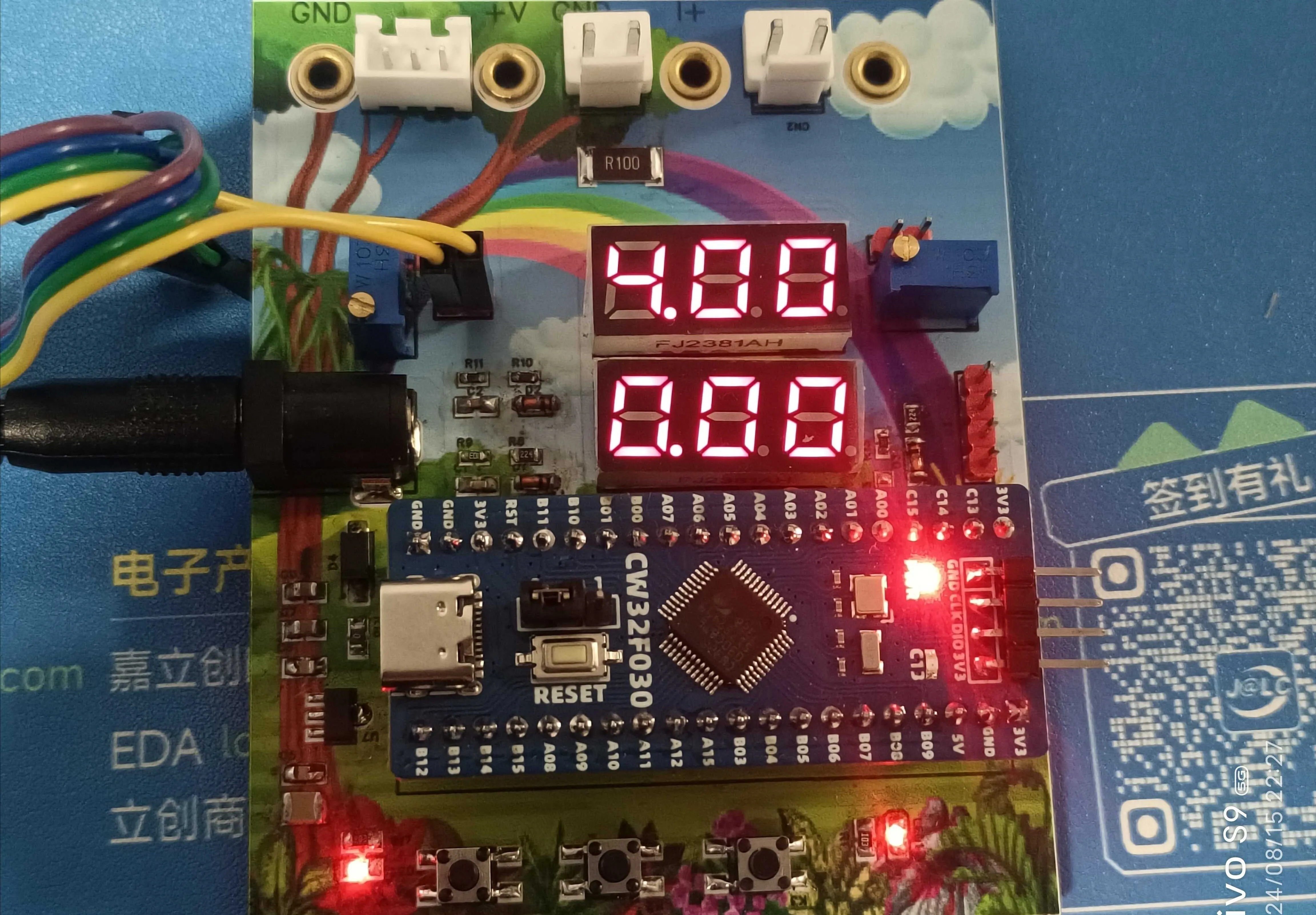
The project uses the LCSC CW32F030C8Tx development board (core board) as the main controller. The key advantages of the CW32 in this project are:
wide operating temperature range (-40~105℃),
wide operating voltage range (1.65V~5.5V, STM32 only supports 3.3V systems),
strong anti-interference capability (HBMESD 8KV), and ESD reliability reaching the highest international standard (STM32 ESD 2KV).
A key feature of this project is a better ADC: a 12-bit high-speed ADC with ±1.0LSB INL 11.3ENOB, multiple Vref reference voltages... (STM32 only supports VDD=Vref),
and stable and reliable eFLASH technology.
The voltage sampling circuit is designed with a voltage divider resistor of 220K+10K, resulting in a voltage division ratio of 22:1 (ADC_IN11).
The maximum voltage to be measured is 30V for safety reasons (the actual maximum display value is 99.9V or 100V).
The current sampling circuit uses a low-side current sampling circuit for current detection. The low-side of the sampling circuit shares a common ground with the development board's meter interface.
The designed sampling current is 3A, and the selected sampling resistor is 100mΩ 1W.
This project uses a digital tube as the display unit. Two 0.28-inch three-digit common-cathode digital tubes are used as display devices. Compared to a display screen, digital tubes offer better visibility and durability in complex environments.
An additional power indicator and I/O operation indicator are designed.
The button control circuit has multiple design options. Thanks to the CW32's internal I/O ports which can be configured with pull-up and pull-down resistors, the external button control circuit does not require configuration. One end of the button is connected to the MCU's I/O, and the other end is grounded. When the button is pressed, the I/O is pulled low.
This project adds an extra TL431 circuit to provide a 2.5V reference voltage, which can be used to provide an external voltage reference for the chip to calibrate the AD converter. From a product design perspective, due to the inherent ADC performance advantages of the CW32, this circuit is unnecessary. This circuit was designed on the development board to learn the relevant application principles.
I followed the official project during a training camp; my hardware knowledge is decent. The software was simply a flashed official firmware. For detailed descriptions and firmware, please see the official link:
https://oshwhub.com/li-chuang-kai-fa-ban/cw32-shu-zi-dian-ya-dian-liu-biao-kai-fa-ban-tao-jian
**Disclaimer: The attached voltage and current meter project is a download from the official website**, link:
https://oshwhub.com/li-chuang-kai-fa-ban/cw32-shu-zi-dian-ya-dian-liu-biao-kai-fa-ban-tao-jian


 京公网安备 11010802033920号

 BY9416


