The circuit shown in Figure 1 is a fully isolated 12-bit, 300 kSPS data acquisition system using only three active devices.
The system operates from a single 3.3 V supply and can handle input signals from 4 mA to 20 mA. Room temperature calibration provides a total error of ±0.06% FSR over a temperature variation of ±10°C, making it ideal for a variety of industrial measurement applications.
The circuit's small size makes this combination an industry-leading solution for 4 mA to 20 mA data acquisition systems where accuracy, speed, cost and size are critical. Data and power are isolated, so the circuit has excellent high voltage tolerance and is immune to ground loop interference common in harsh industrial environments.

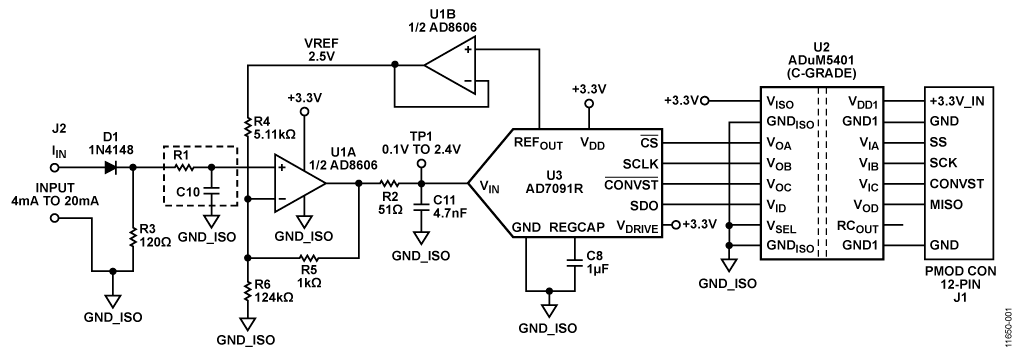
The circuit consists of an input current-to-voltage converter, a level shifting circuit, an ADC stage, and an output isolation stage. The 4 mA to 20 mA input signal is converted into a voltage by resistor R3. With R3 = 120 and an input current of 4 mA to 20 mA, the input voltage to the level shifting circuit is: 0.48 V to 2.4 V. Diode D1 is used to provide protection against accidental reverse connection of the input current source.
The voltage on R3 is level shifted and attenuated by the U1A op amp, which is half the size of the dual AD8606 . The output of the op amp is 0.1 V to 2.4 V, matching the input range of the ADC (0 V to 2.5 V) with a 100 mV headroom to maintain linearity. A buffered voltage reference (VREF = 2.5 V) from the AD7091R ADC is used to generate the required offset. The resistor values can be modified to accommodate other common input ranges described later in this circuit note.
The circuit design supports single power supply. The AD8606 has a minimum rated output voltage of 50 mV (2.7 V supply) and 290 mV (5 V supply) at a load current of 10 mA and a temperature range of -40°C to +125°C. With a 3.3 V supply, load current less than 1 mA, and a narrower temperature range, a conservative estimate of the minimum output voltage is 45 mV to 60 mV.
The circuit design supports single power supply. The AD8606 has a minimum rated output voltage of 50 mV (2.7 V supply) and 290 mV (5 V supply) at a load current of 10 mA and a temperature range of -40°C to +125°C. With a 3.3 V supply, load current less than 1 mA, and a narrower temperature range, a conservative estimate of the minimum output voltage is 45 mV to 60 mV. Taking into account device tolerances, the minimum output voltage (lower end of range) is set to 100 mV to provide a safety margin. The upper limit of the output range is set to 2.4 V to provide 100 mV of headroom for positive swings at the ADC input. Therefore, the nominal output voltage range of the input op amp is 0.1 V to 2.4 V.
The other half of the AD8606(U1B) is used to buffer the internal 2.5 V reference of the AD7091R(U3) analog-to-digital converter.
The AD8606 was chosen for this application because of its low offset voltage (65 V maximum), low bias current (1 pA maximum), and low noise (12 nV/√Hz maximum). At 3.3V supply, power consumption is only 9.2 mW.
The output stage of the op amp is followed by a single-pole RC filter (R2/C11) to reduce out-of-band noise. The cutoff frequency of the RC filter is set to 664 kHz. An optional filter (R1/C10) can be added to further reduce the filter cutoff frequency in the presence of low-frequency industrial noise. In such cases, the sampling rate of the AD7091R can be reduced due to the smaller signal bandwidth.
The AD7091R 12-bit 1 MSPS SAR ADC was chosen because of its ultra-low power consumption of only 349 A at 3.3 V (1.2 mW), which is significantly lower than any competing ADC currently on the market. The AD7091R also has an internal 2.5 V reference with a typical drift of ±4.5 ppm/°C. The input bandwidth is 7.5 MHz, and the high-speed serial interface is SPI-compatible. The AD7091R is available in a small 10-pin MSOP package.
When powered from a 3.3 V supply, the total power dissipation of this circuit (excluding the ADuM5401 isolator) is approximately 10.4 mW. The ADuM5401 quad-channel 2.5 kV isolator integrates a DC/DC converter and is available in a small 16-pin SOIC package. The ADuM5401 consumes approximately 140 mW at a 7 MHz clock frequency. Galvanic isolation is provided by the ADuM5401 quad-channel digital isolator (Grade C). In addition to isolating the output data, the ADuM5401 provides an isolated +3.3 V power supply to this circuit. The ADuM5401 is not required for normal operation of the circuit unless isolation is required. However, the ADuM5401 (Grade C) isolator has a maximum data rate of 25 Mbps, which corresponds to a maximum serial clock frequency of 12.5 MHz. In addition, the SPI port requires that the trailing edge of SCLK drives the output data to the processor, so the total two-way propagation delay of the ADuM5401 (120 ns maximum) limits the upper clock limit to 1/120 ns = 8.3 MHz.
Although the AD7091R is a 12-bit ADC, the serial data is also formatted as 16-bit words to be compatible with the processor serial port requirements. Therefore, the sampling period TS includes the conversion time of the AD7091R650 ns plus 58 ns (additional time required by the data sheet, t1 delay + tQUIET delay), plus 16 clock cycles for the SPI interface data transfer.
T S = 650 ns + 58 ns + 16 × 120 ns = 2628 ns
f S = 1/T S = 1/2628 ns = 380 kSPS
To provide a safety margin, it is recommended to set the SCLK and sample rate to a maximum value of 7 MHz and 300 kSPS respectively. The digital SPI interface can be connected to the microprocessor evaluation board using a 12-pin Pmod compatible connector (Digilent Pmod specification).
circuit design
The circuit shown in Figure 2 provides appropriate gain and level translation to convert a 0.48 V to 2.4 V signal to the ADC input range, which is 0.1 V to 2.4 V.


The transfer function is determined using the superposition principle.


Calculation of Gain and Resistor Values
The gain of the circuit is:

When the input range is 0 mA to 20 mA, the circuit does not require level shifting and the op amp acts as a follower. At this time, the voltage drop on R3 must not exceed the upper limit of the output range (2.4 V). The calculation formula is as follows:
![]()


Now, if you are given the value of one of the three resistors R4, R5, and R6, you can calculate the value of the other two resistors according to Equation 7 and Equation 9. For example, if R5 = 1000 ¬, then R4 = 5,263 ¬ and R6 = 125,310 ¬.
In the actual circuit, resistor values closest to existing standards were chosen for resistors R4 and R6. The selected values are R4 = 5.11k¬ and R6 = 124 k¬.
If these values are chosen carefully, the total error caused by using alternative standard value resistors can be reduced to less than a few percent. However, the output of the U1A op amp at 4 mA and 20 mA input current should be recalculated using Equation 1 to ensure that the required margin is maintained.
The absolute accuracy of such circuits depends primarily on the resistors, so gain and offset calibration is required to eliminate errors due to standard value substitution and resistor tolerances.
Effect of Resistor Temperature Coefficient on Total Error
Equation 1 shows that the output voltage is related to four resistors: R3, R4, R5, and R6. The full-scale output voltage at TP1 is sensitive to small changes in the resistance of each of these four resistors, and its sensitivity is calculated by a simulation program. The input current of the circuit is 20 mA. The calculated sensitivities are SR3= 1.2, SR4= 0.01, SR5= 0.00, SR6= 0.01. Assuming that the temperature coefficients combine in a root-sum-square (rss) fashion, with a 25 ppm/°C resistor for R3 and a 100 ppm/°C resistor for R4, R5, and R6, the total full-scale drift is approximately:
Full-scale drift
= 100 ppm/°C√[(0.25 × S R3 ) 2 + S R4 2 + S R5 2 + S R6 2 )]
= 100 ppm/°C√[(0.25 × 1.2) 2 + 0.01 2 + 0.00 2 + 0.01 2 )]
= 30 ppm/°C
A full-scale drift of 30 ppm/°C corresponds to 0.003%FSR/°C.
Effect of active component temperature coefficient on total error
The DC offset of the AD8606 op amp and AD7091RADC is removed by the calibration procedure.
The offset drift of the AD7091R ADC's built-in reference is 4.5 ppm/°C typical and 25 ppm/°C maximum.
The offset drift of the AD8606 op amp is 1 V/°C typical and 4.5 V/°C maximum.
U1A The error due to the AD8606 input offset is referenced to the input voltage range 2.4 V – 0.48 V = 1.92 V, so it is 2.3 ppm/°C.
The error due to the U1B reference voltage buffer is also approximately 2 ppm/°C based on 2.5 V.
The total drift error result is summarized in Table 1. These errors do not include the ±1 LSB integral nonlinearity error of the AD7091R.
| source of error |
total error |
| Resistance (1%, 100ppm/℃) | ±0.0030%FSR/℃ |
| AD7091R(ΔV V RET )/ΔT=25 ppm/℃ |
±0.0025%FSR/℃ |
|
AD8606, U1A (ΔV OS /ΔT=4.5μV/℃), 2ppm/℃, based on 1.92V |
±0.0002%FSR/℃ |
| AD8606, U1B (μμΔV OS /ΔT=4.5μV/℃, 2ppm/℃, based on 2.5V) |
±0.0002%FSR/℃ |
| Total FSR Error Temperature Coefficient |
±0.0059%FSR/℃ |
| Total %FSR error at ΔT=±10°C |
±0.059%FSR |
Test data before and after two-point calibration
To perform a two-point calibration, first apply 4 mA to the input and record the ADC output code as Code_1. Then, apply a current of 20 mA to the input terminal, and record the ADC output code as Code_2. The gain coefficient is calculated by:

Now, the input current corresponding to any output code Code_x can be calculated by:
![]()
The pre-calibration error is obtained by comparing the ideal transfer function calculated using the nominal values of the components with the uncalibrated actual circuit transfer function. The tolerance of the resistors used in the actual measured circuit is ±1%. Test results do not include temperature changes.
Figure 3 shows the percent error (FSR) test results before and after calibration at ambient temperature. As shown in the figure, the maximum error before calibration is approximately 0.25% FSR. After calibration, the error is reduced to ±0.02% FSR, which is roughly equivalent to the 1 LSB error of the ADC.


PCB layout considerations
In any circuit where precision is important, power and ground return layout on the circuit board must be carefully considered. The PCB should isolate the digital and analog parts as much as possible. The PCB of this system is made of a simple double-layer board stack, but better EMS performance can be obtained by using a 4-layer board. For information on layout and grounding, see the MT-031 guide. For information on decoupling techniques, see the MT-101 guide . The AD8606 power supply should be decoupled with 10 ¬F and 0.1 ¬F capacitors for proper noise suppression and ripple reduction. These capacitors should be as close as possible to the corresponding device, and the 0.1 ¬F capacitors should have low ESR values. For all high frequency decoupling, ceramic capacitors are recommended. Power traces must be as wide as possible to provide a low impedance path and reduce the effects of glitches on the power lines. The ADuM5401isoPower integrated DC/DC converter requires power supply bypassing on the input and output power pins. Note that low ESR bypass capacitors are required between Pins 1 and 2 and between Pins 15 and 16, and these should be placed as close to the chip pads as possible.
To suppress noise and reduce ripple, at least two capacitors need to be connected in parallel. For VDD1 and VISO, the recommended capacitor values are 0.1 ¬F and 10 ¬F. Smaller capacitors must have low ESR, ceramic capacitors are recommended. The total trace length from the end of the low ESR capacitor to the input power pin must not exceed 2 mm. If the bypass capacitor trace length exceeds 2 mm, data may be corrupted. Consider bypassing between Pin 1 and Pin 8 and Pin 9 and Pin 16 unless the two common ground pins are tied together close to the package. See the ADuM5401 data sheet for more information.
For a complete documentation package, including schematics, board layout, and bill of materials (BOM), please refer to: www.analog.com/CN0336-DesignSupport.
High voltage capability
This PCB is designed according to the 2500 V basic insulation specification. High voltage testing above 2500 V is not recommended. Caution must be exercised when using this evaluation board at high voltages, and this PCB must not be relied upon for safety functions as it has not been high potential tested (also known as high voltage testing or withstand voltage insulation testing) and has not been safety certified.


Blockdiagram
All reference designs on this site are sourced from major semiconductor manufacturers or collected online for learning and research. The copyright belongs to the semiconductor manufacturer or the original author. If you believe that the reference design of this site infringes upon your relevant rights and interests, please send us a rights notice. As a neutral platform service provider, we will take measures to delete the relevant content in accordance with relevant laws after receiving the relevant notice from the rights holder. Please send relevant notifications to email: bbs_service@eeworld.com.cn.
It is your responsibility to test the circuit yourself and determine its suitability for you. EEWorld will not be liable for direct, indirect, special, incidental, consequential or punitive damages arising from any cause or anything connected to any reference design used.
Supported by EEWorld Datasheet
EEWorld
subscription
account

EEWorld
service
account

Automotive
development
community

Robot
development
community

About Us Customer Service Contact Information Datasheet Sitemap LatestNews


Room 1530, 15th Floor, Building B,
No.18 Zhongguancun Street,
Haidian District,
Beijing, Postal Code: 100190
China
Telephone: 008610 8235 0740
 京公网安备 11010802033920号

 EL1C221KT


