This circuit is a complete implementation of the analog part of a broadband direct conversion transmitter (analog baseband input, RF output). This circuit supports RF frequencies ranging from 500 MHz to 4.4 GHz through the use of a phase-locked loop (PLL) and a wideband integrated voltage-controlled oscillator (VCO). Harmonic filtering from the PLL local oscillator (LO) ensures excellent quadrature accuracy, sideband suppression and low EVM.


Low-noise, low-dropout regulators (LDOs) ensure that the power management scheme has no adverse impact on phase noise and EVM. This combination of devices provides industry-leading direct conversion transmitter performance from 500 MHz to 4.4 GHz.
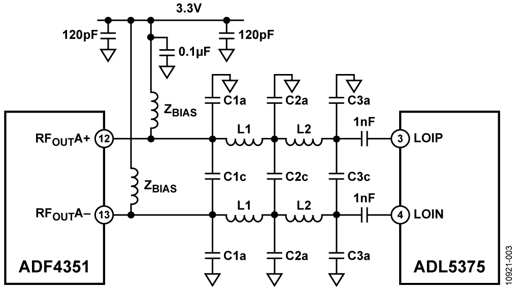
The circuit shown in Figure 1 uses a fully integrated fractional-N PLL IC ADF4351 and a wideband transmit modulator ADL5375 . The ADF4351 provides the LO signal to the transmit quadrature modulator ADL5375, which upconverts the analog I/Q signal to an RF signal. Together, the two devices provide a wideband baseband I/Q to RF transmit solution. The ADF4351 is powered by an ultralow noise 3.3 V ADP150 regulator for optimal LO phase noise performance. The ADL5375 is powered by a 5 V ADP3334 LDO. The ADP150 LDO's output voltage noise is only 9 μV rms, helping to optimize VCO phase noise and reduce the effects of VCO pushing (equivalent to power supply rejection).
The ADF4351 RF output needs to be filtered to attenuate the harmonic levels and minimize the error of the ADL5375 quadrature generation module. According to measurements and simulations, it is known that odd-order harmonics contribute more to quadrature error than even-order harmonics; if odd-order harmonics are attenuated below −30 dBc, sideband suppression performance of −40 dBc or better can be achieved . The ADF4351 data sheet gives its second harmonic (2H) and third harmonic (3H) levels as shown in Table 1.
To get the third harmonic below −30 dBc, approximately 20 dB of attenuation is required.
| Harmonic components |
Value (dBc) |
describe |
| second |
-19 |
Fundamental VCO output |
| third |
-13 |
Fundamental VCO output |
| second |
-20 |
Divided VCO output |
| third |
-10 |
Divided VCO output |
This circuit offers four different filter options to suit four different frequency bands. These filters are designed with a 100 Ω differential input (ADF4351 RF output properly matched) and a 50 Ω differential output (ADL5375 LOIN differential impedance). And use the Chebyshev response to get the best filter roll-off, but the ripple in the passband will be increased.
The schematic diagram of the filter is shown in Figure 3. This topology is flexible and can use a fully differential filter to minimize component count, a single-ended filter for each output, or a combination of the two. We found that for higher frequencies (>2 GHz), the series inductance value of two single-ended filters is twice the inductance value of a fully differential filter, thus reducing the impact of device parasitics and providing optimal performance. For lower frequencies (<2 GHz), fully differential filters are sufficient.
The ADF4351 output matching includes the Z BIAS pull-up resistor, and the decoupling capacitor of the power node also plays a role. To achieve broadband matching, it is recommended to use a resistive load (Z BIAS = 50 Ω) or to connect a resistive load in parallel with the reactive load of Z BIAS . The latter provides slightly higher output power, depending on the inductor chosen. Note that the shunt resistor can be placed at C1c as a differential component (i.e., 100 Ω) to minimize board space (see Type B filter in Table 2).
Design the filter so that the cutoff frequency is approximately 1.2 to 1.5 times the highest frequency in the band of interest. This cutoff frequency allows some margin in the design because typically the cutoff frequency will be lower than the design value due to parasitic effects. Printed circuit board (PCB) parasitics can be simulated in electromagnetic (EM) simulation tools for improved accuracy.

| Frequency range(MHz) |
Z BIAS |
L1(nH) |
L2(nH) |
C1a(pF) |
C1c(pF) |
C2a(pF) |
C2c(pF) |
C3a(pF) |
C3c(pF) |
| 500 to 1300 (Type A filter) |
27nH||50Ω |
3.9 |
3.9 |
DNI |
4.7 |
DNI |
5.6 |
DNI |
3.3 |
| 850 to 2450 (Type B filter) |
19 nH||(100Ω, position C1c) |
2.7 |
2.7 |
3.3 |
100Ω |
4.7 |
DNI |
3.3 |
DNI |
| 1250 to 2800 (filter type C) |
50Ω |
0Ω |
3.6 |
DNI |
DNI |
2.2 |
DNI |
1.5 |
DNI |
| 2800 to 4400 (filter type D) |
3.9nH |
0Ω |
0Ω |
DNI |
DNI |
DNI |
DNI |
DNI |
DNI |
As can be seen from Table 2, at lower frequencies below 1250 MHz, a fifth-order filter is required. For frequencies from 1.25 GHz to 2.8 GHz, a third-order filter is sufficient. For frequencies above 2.8 GHz, filtering is not required because the harmonic levels are very low and sufficient to meet sideband suppression requirements.


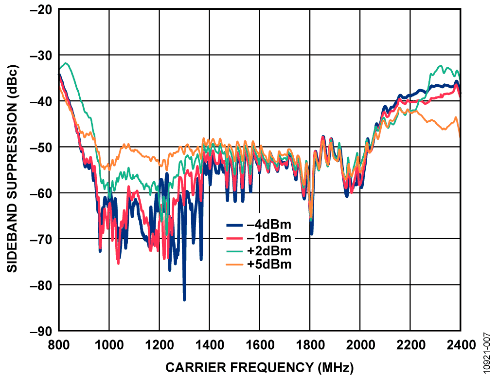
For a circuit using a Type B filter (800 MHz to 2,400 MHz), the sideband suppression performance versus frequency is shown in Figure 4. The test conditions for this scan are as follows:
EVM is a measure of the performance quality of a digital transmitter or receiver, reflecting the deviation of actual constellation points from their ideal positions due to amplitude and phase errors (see Figure 5).
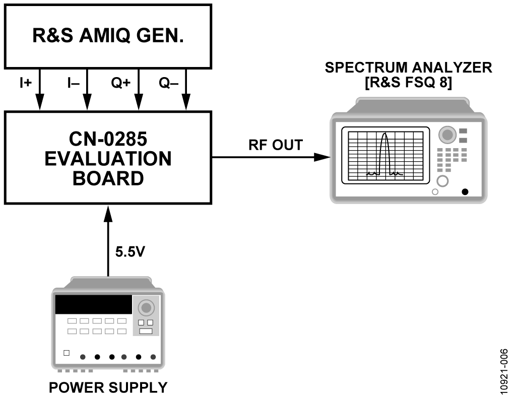
Table 3 shows the EVM measurement results with and without filter. In this example, the baseband I/Q signal is generated from the differential I and Q analog outputs using 3GPP test model 4 using a Rhode & Schwarz AMIQ I/Q modulation generator. A type B filter is also used. Figure 6 is a block diagram of the EVM test setup. For comparison, the ADF4350 was also measured. The lower EVM of the ADF4351 due to improved in-band PLL noise performance can be seen in Table 3. Other factors that improve EVM include the ADF4351's lower phase frequency detector (PFD) spurious levels.
| Frequency(MHz) |
ADF4350 composite EVM, no LO filtering |
ADF4350 composite EVM, with LO filter, filter B |
ADF4351 composite EVM, with LO filter, filter B |
| 2140 |
3.27% |
1.31% |
1.02% |
| 1800 |
1.46% |
1.13% |
0.95% |
| 900 |
10.01% |
1.03% |
0.96% |

Driving the ADL5375 LO input differentially provides performance benefits in addition to improved sideband suppression and EVM. This advantage improves the modulator output OIP2 performance by 2 dB to 5 dB compared to a single-ended LO drive. Note that most external VCOs only provide single-ended outputs, so using a differential output with the ADF4351 is preferable to using an external VCO.
Figure 7 shows the sideband suppression results using an 850 MHz to 2450 MHz filter (Type B filter).

For the complete design support package for this circuit note, see http://www.analog.com/CN0285-DesignSupport .


Blockdiagram
All reference designs on this site are sourced from major semiconductor manufacturers or collected online for learning and research. The copyright belongs to the semiconductor manufacturer or the original author. If you believe that the reference design of this site infringes upon your relevant rights and interests, please send us a rights notice. As a neutral platform service provider, we will take measures to delete the relevant content in accordance with relevant laws after receiving the relevant notice from the rights holder. Please send relevant notifications to email: bbs_service@eeworld.com.cn.
It is your responsibility to test the circuit yourself and determine its suitability for you. EEWorld will not be liable for direct, indirect, special, incidental, consequential or punitive damages arising from any cause or anything connected to any reference design used.
Supported by EEWorld Datasheet
EEWorld
subscription
account

EEWorld
service
account

Automotive
development
community

Robot
development
community

About Us Customer Service Contact Information Datasheet Sitemap LatestNews


Room 1530, 15th Floor, Building B,
No.18 Zhongguancun Street,
Haidian District,
Beijing, Postal Code: 100190
China
Telephone: 008610 8235 0740
 京公网安备 11010802033920号

 KST5401