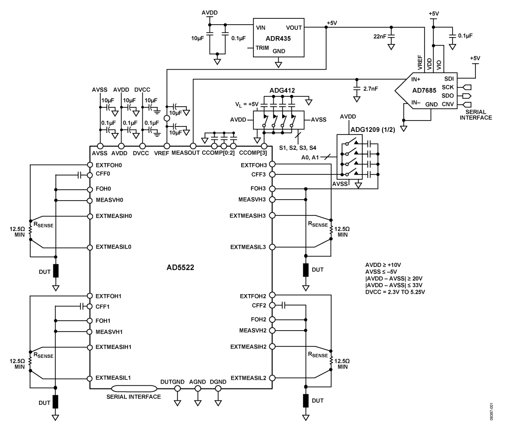
This circuit consists of a four-channel parametric measurement unit (PMU) and supporting devices for a minimum of four device under test (DUT) channels. PMU channels are usually shared by several DUT channels. Although the AD5522 is highly integrated and provides a complete four-channel PMU solution, it still requires at least an external reference voltage source and an ADC to form the ATE signal chain. The reference and ADC are often shared among multiple PMU packages. To further increase flexibility, external switches can be added to expand the capabilities of the PMU by extending the range of DUT capacitances that the AD5522 can drive.

The four-channel PMU AD5522 can provide forcing functions and measurement functions for the DUT, but digital processing is required outside the PMU. This can be achieved by:
Using the internal disable function of each MEASOUTx pin, multiple channels can share one ADC. This requires writing commands to the PMU registers to enable/disable the corresponding switches. If you choose this method, you should note that only one MEASOUTx channel can be selected at a time.
Alternatively, an external 4:1 multiplexer can be used to control measurement channel selection. In this way, all four MEASOUTx paths can be enabled, with the measurement channel selected by the multiplexer. Similarly, using an 8:1 or 16:1 multiplexer allows more measurement paths to share one ADC. The choice of multiplexer will depend on the ADC used and its input voltage range. For bipolar input ADCs, the ADG1404 / ADG1204 family of devices would be ideal; if using a single supply, the ADG706 and ADG708 are more suitable. In addition to the switch impedance, the output impedance of the MEASOUTx path is typically 60 Ω. Therefore, an ADC buffer such as the ADA4898-1 should be considered to drive the ADC (buffer not shown in the figure).
The AD7685, 16-bit, 250 kSPS ADC is capable of handling the 0 V to 4.5 V output range of the MEASOUTx path, making it suitable for this application. Additionally, if an upgrade path is desired, other ADCs that are faster but the same size, such as the 16-bit, 500 kSPS AD7686 , are also attractive options.
If a 20 V output range is required, the AD5522 requires a 5 V reference. The ADR435 5 V XFET reference was chosen because of its low temperature coefficient (10 ppm/°C for Grade A; 3 ppm/°C for Grade B) and low noise (8 μV peak-to-peak, 0.1 Hz to 10 Hz ) and the ability to drive multiple PMU channels (30 mA source current, 20 mA sink current) features.
Some applications require the PMU to be able to drive various sizes of DUT capacitors, especially in applications where the PMU is connected to a power supply pin, or where the PMU is used as a device power supply and the DUT's decoupling/bypass capacitance is present. In this case, connecting an external switch to the CCOMP pin instead of a fixed capacitor allows the additional CCOMP capacitor to be turned on or off, optimizing settling time and stability under various capacitive load conditions. The switch selected for this circuit is the four-channel SPST switch ADG412, whose on-resistance is less than 50 Ω. Since most multiplexers only allow one of multiple channels to be on at a time, a four-channel SPST switch was chosen instead of a multiplexer. With a four-channel switch, the drains can be connected together and the sources can be connected to compensation capacitors, providing 24 − 1 possible CCOMP combinations.
Likewise, this circuit uses the ADG1209 differential multiplexer to accommodate a wider range of feedforward capacitances connected to the CFFx pins, allowing the AD5522 to drive a wider range of DUT capacitances. Use a multiplexer with series resistance such that 1/(2π × R ON × C DUT ) > 100 kHz. In this example, the ADG1209 is used to switch the two channels of the AD5522.
The switch and capacitor will experience a voltage offset within the same voltage range as the AD5522 FOH pin. Therefore, the voltage ratings of switches and capacitors should take this into account. CFF capacitors can have tolerances of 10% or less, and this additional variable directly affects settling time, especially in current mode when measuring low currents. The selected CCOMP capacitor tolerance should be no greater than 5%. Table 1 lists the recommended nominal values of the compensation capacitors CCOMP and CFF for different load capacitances.
| CLOAD | CCOMP | CFF |
| ≤1nF | 100pF | 220pF |
| ≤10 nF | 100pF | 1nF |
| ≤100 nF | C LOAD /100 | C LOAD /10 |
This circuit must be built on a multilayer circuit board with a large area ground plane. For optimal performance, proper layout, grounding, and decoupling techniques must be used (refer to Tutorial MT-031 - "Grounding Data Converters and Unraveling the Mysteries of AGND and DGND", and Tutorial MT-101 - "Decoupling Technology "). Please note that Figure 1 is a schematic diagram and does not show all required decoupling.
Careful consideration of power and ground return layout helps ensure rated performance is achieved. The printed circuit board (PCB) used to install the AD5522 should be designed to separate the analog and digital parts and be limited to a certain area of the circuit board. If the AD5522 is in a system with multiple devices that require an AGND to DGND connection, the connection can only be made at one point. Place the star ground point as close to the device as possible.


For power supplies with multiple pins (AV SS and AV DD ), it is recommended to tie the pins together and decouple each power supply only once.
The AD5522 should have sufficiently large 10 µF power supply decoupling capacitors in parallel with the 0.1 µF capacitors on each supply and as close as possible to the package, ideally directly opposite the device. The 10 μF capacitor is a tantalum bead type capacitor. The 0.1 µF capacitor should have low effective series resistance (ESR) and low effective series inductance (ESL)—this is typically the case with common ceramic-type capacitors that provide a low-impedance path to ground at high frequencies, capable of handling transient currents caused by internal logic switching .
Avoid routing digital lines underneath the device as this will couple noise into the device. However, the analog ground plane can be placed below the AD5522 to avoid noise coupling (this practice only applies to packages with pads facing up). The power supply lines to the AD5522 should be traced as wide as possible to provide a low impedance path and reduce the effects of surges on the power lines. Fast-switching digital signals should be shielded with digital ground to avoid radiating noise to other devices on the board, and should never be located close to the reference input. Noise on all VREF lines must be minimized.
Overlapping of digital and analog signals should be avoided. Traces on opposite sides of the board should be perpendicular to each other to reduce feedthrough effects on the board. Like all low-profile packages, bending of the package must be avoided, and point loads on the package surface must be avoided during assembly.
Also note that the exposed pad of the AD5522 is connected to the negative supply AV SS .


Blockdiagram
All reference designs on this site are sourced from major semiconductor manufacturers or collected online for learning and research. The copyright belongs to the semiconductor manufacturer or the original author. If you believe that the reference design of this site infringes upon your relevant rights and interests, please send us a rights notice. As a neutral platform service provider, we will take measures to delete the relevant content in accordance with relevant laws after receiving the relevant notice from the rights holder. Please send relevant notifications to email: bbs_service@eeworld.com.cn.
It is your responsibility to test the circuit yourself and determine its suitability for you. EEWorld will not be liable for direct, indirect, special, incidental, consequential or punitive damages arising from any cause or anything connected to any reference design used.
Supported by EEWorld Datasheet
EEWorld
subscription
account

EEWorld
service
account

Automotive
development
community

Robot
development
community

About Us Customer Service Contact Information Datasheet Sitemap LatestNews


Room 1530, 15th Floor, Building B,
No.18 Zhongguancun Street,
Haidian District,
Beijing, Postal Code: 100190
China
Telephone: 008610 8235 0740
 京公网安备 11010802033920号

 1.5KE100A-A


