Summary of I2C basics: How does I2C communication actually work?
Source: InternetPublisher:风向双子座 Keywords: I2C I2C communication Updated: 2025/02/14
I2C communication is short for Inter-Integrated Circuit, which is a communication protocol developed by Philips Semiconductors for transmitting data between a central processing unit and multiple ICs on the same circuit board using only two common wires.
Due to its simplicity, it is widely used for communication between microcontrollers and sensor arrays, displays, IoT devices, EEPROMs, etc.
This is a synchronous serial communication protocol. This means that the data bits are transmitted one by one at regular time intervals set by a reference clock line.
1. Characteristics of I2C
Following are some important features of I2C communication protocol:
(1) Only two common buses (wires) are needed to control any device/IC on the I2C network;
(2) There is no need to agree on the data transmission rate in advance like UART communication. Therefore, the data transmission speed can be adjusted at any time as needed;
(3) A simple mechanism for verifying transmitted data;
(4) Use a 7-bit addressing system to locate a specific device/IC on the I2C bus;
(5) The I2C network is easy to expand, and new devices can be simply connected to two common I2C buses.
2. I2C Hardware
1. Physical I2C bus
The I2C bus (interface lines) consists of only two wires, called the serial clock line (SCL) and the serial data line (SDA). The data to be transmitted is sent over the SDA line and is synchronized with the clock signal from SCL. All devices/ICs on the I2C network are connected to the same SCL and SDA lines, as shown below:
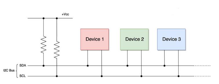
Both I2C buses (SDA, SCL) are used as open-drain drivers. This means that any device/IC on the I2C network can drive SDA and SCL low, but cannot drive them high. Therefore, each bus uses a pull-up resistor to hold them high (positive voltage) by default.
The reason for using an open-drain system is that there is no possibility of a short circuit, which can occur when one device tries to pull the line high while the other tries to pull it low.
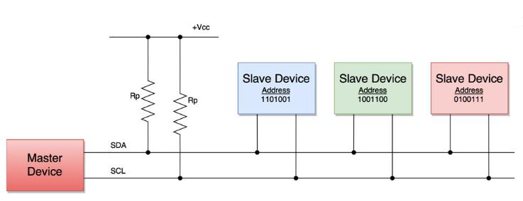
2. Master and Slave Devices
Devices connected to the I2C bus are either master or slave. At any given moment, only one master device is active on the I2C bus. It controls the SCL clock line and decides what to do on the SDA data line.
All devices that respond to instructions from the master are slaves. In order to distinguish multiple slave devices connected to the same I2C bus, each slave device is physically assigned a permanent 7-bit address.
When the master device wants to transfer data to or from a slave device, it specifies this particular slave device address on the SDA line and then proceeds with the transmission. Thus, effective communication takes place between the master device and a particular slave device.
All other slave devices will not respond unless their address is specified by the master on the SDA line.
3. Data transmission protocol
The master and slave devices follow the following protocol (set of rules) to transfer data between them.
Data is transferred between the master and slave devices over a single SDA data line, through a pattern sequence of 0s and 1s (bits). Each sequence of 0s and 1s is called a transaction, and the data in each transaction is structured as follows:
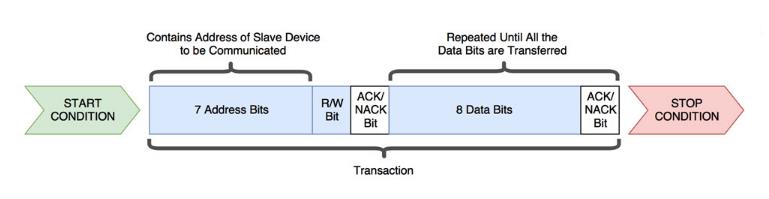
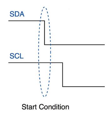
1. Starting conditions
Whenever the master device/IC decides to start a transaction, it switches the SDA line from a high voltage level to a low voltage level before switching the SCL line from a high voltage level to a low voltage level.
Once the master sends the start condition, all slaves become active even if they are in sleep mode and wait for the address bit.
2. Address Block
It consists of 7 bits and is filled with the slave address to which the master needs to send/receive data. All slave devices on the I2C bus compare these address bits with their address.
3. Read/write bit
This bit specifies the direction of data transfer. If the master device/IC needs to send data to the slave device, this bit is set to "0". If the master IC needs to receive data from the slave device, it is set to "1".
4. ACK/NACK bit
It stands for Acknowledged/Unacknowledged bit. If the physical address of any slave device coincides with the address broadcasted by the master device, the value of this bit is set to "0" by the slave device. Otherwise it remains at logic "1" (default).
5. Data Block
It consists of 8 bits, which are set by the sender, the data bits that need to be transmitted to the receiver. This block is followed by an ACK? ? /NACK bit, which the receiver sets to '0' if the receiver has successfully received the data. Otherwise it remains at logic '1'.
This combination of a data block followed by an ACK/NACK bit is repeated until the data is completely transmitted.
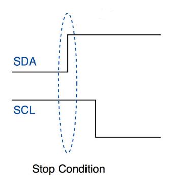
6. Stop Condition
After transmitting the required block of data over the SDA line, the master device switches the SDA line from low to high and then switches the SCL line from high to low.
Note: A logic '0' or setting a bit to '0' is equivalent to applying a low voltage on the SDA line and vice versa.
4. How does I2C communication actually work?
I2C communication/transaction is initiated by the master device to send data to or receive data from the slave device. Let us understand in detail how these two scenarios work.
1. Send data to the slave device
When a master device attempts to send data to a specific slave device over the I2C bus, the following sequence of operations occurs:
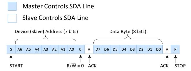
(1) The master device sends the start condition;
(2) The master device sends the 7 address bits corresponding to the target slave device;
(3) The master device sets the read/write bit to "0", indicating writing;
(4) There are now two possibilities: If no slave device matches the address sent by the master, the next ACK? /NACK bit remains at "1" (default). This signals to the master that the slave device identification was unsuccessful. The master clock will end the current transaction by sending a stop condition or a new start condition. If there is a slave device with the same address as the master device, the slave device will set the ACK/NACK bit to "0", which signals to the master that the slave device has been successfully located.
(5) If the slave device is successfully located, the master device now sends 8 bits of data, which are only considered and received by the target slave device. This data has no meaning to the remaining slave devices.
(6) If the data is successfully received by the slave device, it sets the ACK/NACK bit to “0”, which indicates to the master device to continue.
(7) Repeat the first two steps until all data is transmitted.
(8) After all data is sent to the slave devices, the master device sends a stop condition to notify all slave devices that the current transaction has ended.
The following diagram represents the overall data bits sent on the SDA line and the devices that control each bit:
2. Read data from the slave device
The order of operations is the same as in the previous scenario, except for the following:
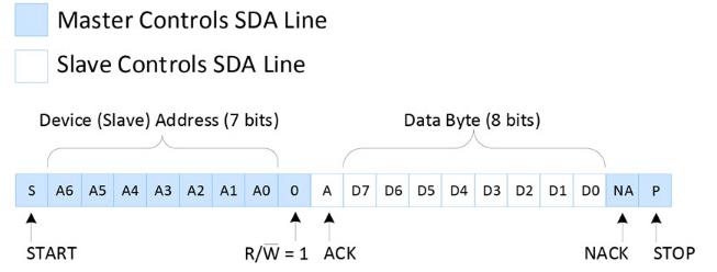
(1) The master sets the read/write bit to "1" instead of "0", which signals to the target slave that the master is waiting for data from it;
(2) The 8 bits corresponding to the data block are sent by the slave device, and the ACK/NACK bit is set by the master device;
(3) Once the master device receives the required data, it sends a NACK bit. The slave device then stops sending data and releases the SDA line.
If the master device reads data from a specific internal location of the slave device, it first sends the location data to the slave device using the steps in the previous scenario. It then begins the process of reading the data with a repeated start condition.
The following diagram represents the overall data bits sent on the SDA line and the devices that control each bit:
3. The concept of clock stretching
Assume that the master device initiates a transaction and sends the address bit of a specific slave device, followed by a read bit of "1". The specific slave device is required to send an ACK bit, followed by the data.
But if the slave takes some time to get and send data to the master, during this gap the master will think that the slave is sending some data.
To prevent this, the slave device holds the SCL clock line low until it is ready to transmit a data bit. By doing this, the slave device signals the master device to wait for a data bit until the clock line is released.
- What is a quartz crystal? Quartz crystal equivalent circuit analysis
- LM337 pin diagram and parameters, LM337 application circuit diagram
- How do pull-up resistors work? How do I choose a pull-up resistor value?
- What is a pure resistance circuit? What is a pure resistance AC circuit?
- Types and structures/characteristics/functions/implementations of smart sensors
- Causes and solutions for noise in digital Class D amplifiers
- Advantages and disadvantages of organic semiconductors, the conductive mechanism of organic semiconductors
- Working principle and truth table of JK flip-flop
- Share a Motorola amplifier circuit
- Introduction of TDA4863J/4863AJ TV field scanning IC
- I2C address switching circuit
- 555 square wave oscillation circuit
- 555 photo exposure timer circuit diagram
- Introducing the CD4013 washing machine timer circuit diagram
- Simple level conversion circuit diagram
- 555 electronic guide speaker circuit diagram for blind people
- Circuit diagram of disconnection alarm composed of 555
- Analog circuit corrector circuit diagram
- color discrimination circuit
- Color sensor amplification circuit


 京公网安备 11010802033920号