FPGA Features and Architecture
Source: InternetPublisher:supremeOne Keywords: fpga programmable device Updated: 2025/01/16
FPGA (Field Programmable Gate Array) is a product that is further developed on the basis of programmable devices (such as PAL, GAL, CPLD, etc.). It is developed as a semi-custom circuit in the field of ASIC, which not only solves the shortcomings of custom circuits, but also overcomes the limitations of the original programmable device gate circuit. It is the main hardware platform for digital system design today. Its main feature is that users can configure and program it completely through software to complete specific functions. And it can be erased repeatedly.
In modification and upgrading, there is no need to make additional changes to the PCB circuit board, but only to modify and update the program in the computer, making the hardware design work become software development work. This shortens the system design cycle, improves the flexibility of implementation, and reduces costs.
Characteristics of FPGA
1. High performance and real-time performance
Since FPGA chips are implemented by millions of logic units, they have parallel processing capabilities and run much faster than microcontrollers and DSPs.
2. High integration performance
FPGA can embed hard/soft IP cores internally according to user needs to meet different requirements. The use of SOPC technology can save the area of the target hardware.
3. High reliability and low cost
Today's FPGA chips are 100% tested before leaving the factory, which means that designers do not need to bear the production costs of the chips.
4. High flexibility and low power consumption
FPGA is field programmable. Users can repeatedly program, erase, use or use different designs to implement different functions, while the peripheral circuit remains unchanged. This brings great convenience to product upgrades and maintenance.
FPGA Architecture
FPGA uses the concept of logic cell array (LCA), which includes configurable logic modules CLB (Configurable Logic Block), input/output blocks (IOB), interconnects and static memory SRAM for storing programming data.
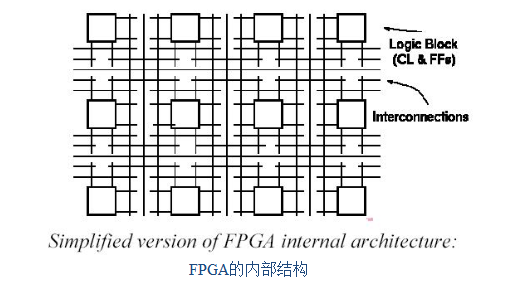
1. Programmable logic module load balancing
CLB is the basic unit of logic function, usually arranged in a regular array and scattered throughout the chip. Load balancing generally consists of logic function generators, triggers, data selectors, etc. Function generators are used to implement any combination of n input variables.
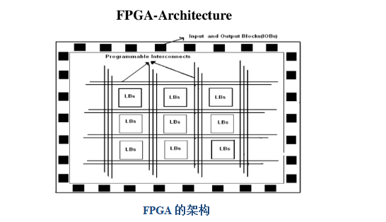
2. Input/Output Module (IOB)
IOB provides connection between device pins and internal logic array, mainly composed of input generator, input buffer, output trigger/latch and output buffer, which can be defined as input/output with bidirectional I/O function. When defined as input, the signal through the pin is first sent to the input buffer, which is divided into two channels, one is sent directly to the MUX channel, and the other is sent to the input path D flip-flop after a delay. Then it is sent to the data selector, which determines whether the CLB array is sent to the input buffer or triggered according to different control information.
3. Programmable interconnection resources infrared
IR can be connected between CLB and CLB or between CLB and IOB. IR is mainly composed of many metal segments. These metal segments have programmable switches and can connect various circuits through automatic wiring. The internal lines of the chip are divided by length: single-length line (a), double-length line (b) and long line (c).
- An article explains the working principle of the Wheatstone bridge
- What is a pure resistance circuit? What is a pure resistance AC circuit?
- How does sand become chips?
- Advantages and disadvantages of organic semiconductors, the conductive mechanism of organic semiconductors
- Datasheet/Pinout/Technical Specifications of LMC555
- Basic characteristics/working principles and application circuits of tunnel diodes
- What is the difference between high-side and low-side resistive current sensing
- Introduction of TDA4863J/4863AJ TV field scanning IC
- LED lights that “drain” battery power
- Purpose and composition of amplifier circuit: low frequency voltage amplifier amplifier circuit
- The accuracy of DC-DC power supply is becoming more and more precise with the accuracy of FPGA.
- What are the design specifications for FPGA power supply design?
- Low jitter standard clock buffer, did you know?
- Design of circuit module of fingerprint identification system based on FPGA
- Design based on FPGA configuration circuit
- Fingerprint identification system circuit diagram based on FPGA
- 555 square wave oscillation circuit
- 555 photo exposure timer circuit diagram
- Introducing the CD4013 washing machine timer circuit diagram
- Simple level conversion circuit diagram


 京公网安备 11010802033920号