Precise long delay circuit designed using CD4060
Source: InternetPublisher:已注销 Keywords: Delay circuit Updated: 2023/12/11
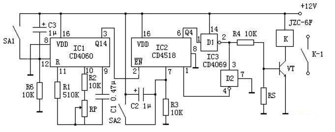
This circuit consists of CD4060 as the time base circuit of the timer. The timing time base pulse generated by the circuit is divided by the internal frequency divider and then outputs the time base signal. After dividing the frequency through the peripheral frequency dividing circuit, the required timing control time is obtained.
1. Circuit working principle
The circuit principle is shown in the figure below. After power-on, the time base oscillator oscillates and outputs the time base signal after frequency division. IC2 as a frequency divider starts counting the frequency division. When the count reaches 10, Q4 outputs a high level, which is inverted by D1 and changes to a low level to cut off VT. The relay is powered off and released, cutting off the working power of the controlled circuit. At the same time, the low level output of D1 is inverted by D2 to a high level and then added to the CP terminal of IC2, so that the high level output of the output terminal is maintained.
After the circuit is powered on to reset IC1 and IC2, the four output terminals of IC2 are all low level. The low level output by Q4 is inverted by D1 and becomes a high level. VT is turned on through R4, and the relay is energized to absorb the sum. This working state is the power-on and timed-off state.
2. Component selection
IC1 uses CD4060, IC2 uses CD4518, and IC3 uses CD4069; VT1 uses 9013 and 9014; C1 uses ceramic capacitors, and C2 and C3 use aluminum electrolytic capacitors with a withstand voltage of 15V; the relay uses model JZC-6F DC relay; RP uses 200K ordinary Adjustable potentiometer; the resistor is a 1/8 or 1/4W metal film resistor, and SA1 and SA2 are small toggle switches.
3. Production and debugging methods
If you want to change the power-on, disconnection and timing status, you can add a first-level inverter between the output terminals D1 and VT. The length of the timing time can be adjusted through RP, or it can be changed by connecting to the output end of IC2 according to the binary-decimal coding correspondence. The timing range of the circuit in this example is: 3min~1h.
- Semiconductor fuse symbol diagram, semiconductor fuse working principle, how to select semiconductor fuse
- LM338 pin diagram and function, LM338 schematic diagram, LM338 application circuit diagram
- RISC structure and its advantages and disadvantages
- Analysis of Operational Amplifier Differentiator Circuit
- What is a photocoupler and how to select and use one?
- The unidirectional conduction current of the diode, the diode and its common uses
- Voltage divider circuit calculation formula, where to find the voltage divider circuit?
- How do pull-up resistors work? How do I choose a pull-up resistor value?
- Which TVS diodes are suitable for RS232/RS485 and Controller Area Network applications?
- Datasheet/Pinout/Technical Specifications of LMC555
- One of the long delay circuits using integrated circuits
- The third delay circuit using 555 time base integrated circuit
- Thyristor cut-off delay circuit 6
- Conductive tube controlled charging delay circuit
- One of the lighting delay circuits using transistors
- High sensitivity acoustic vibration alarm circuit
- Logic signal long delay circuit
- Power frequency 0-5 minute delay circuit diagram
- Low voltage contactor instantaneous voltage loss and undervoltage delay circuit
- 555 cascade long delay circuit


 京公网安备 11010802033920号